

Semiconductor device
- Summary
- Abstract
- Description
- Claims
- Application Information
AI Technical Summary
Benefits of technology
Problems solved by technology
Method used
Image

Examples
first embodiment
[0085]A semiconductor device according to a present embodiment is an ultrasonic transducer (ultrasonic transmitting / receiving sensor) manufactured using, for example, a MEMS (Micro Electro Mechanical System) technique.
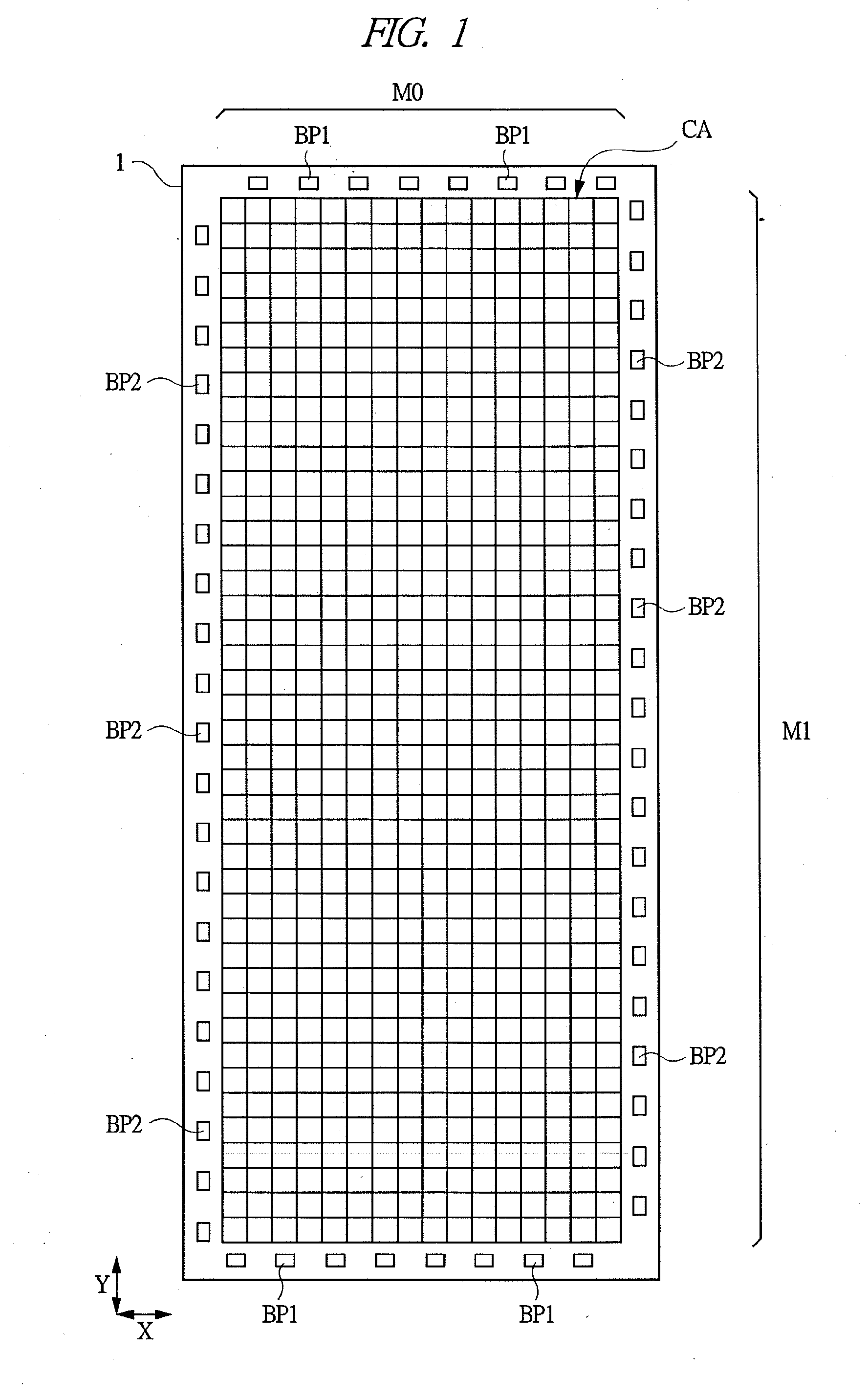
[0086]FIG. 1 is a total plan diagram of a semiconductor chip 1 configuring the semiconductor device according to the present embodiment.
[0087]The semiconductor chip 1 comprises a first main surface (upper surface, front surface) and a second main surface (lower surface, rear surface) positioned so as to be opposite to each other along a thickness direction. FIG. 1 shows a plan diagram on a first main surface side (that is, an upper surface diagram) of the semiconductor chip 1.
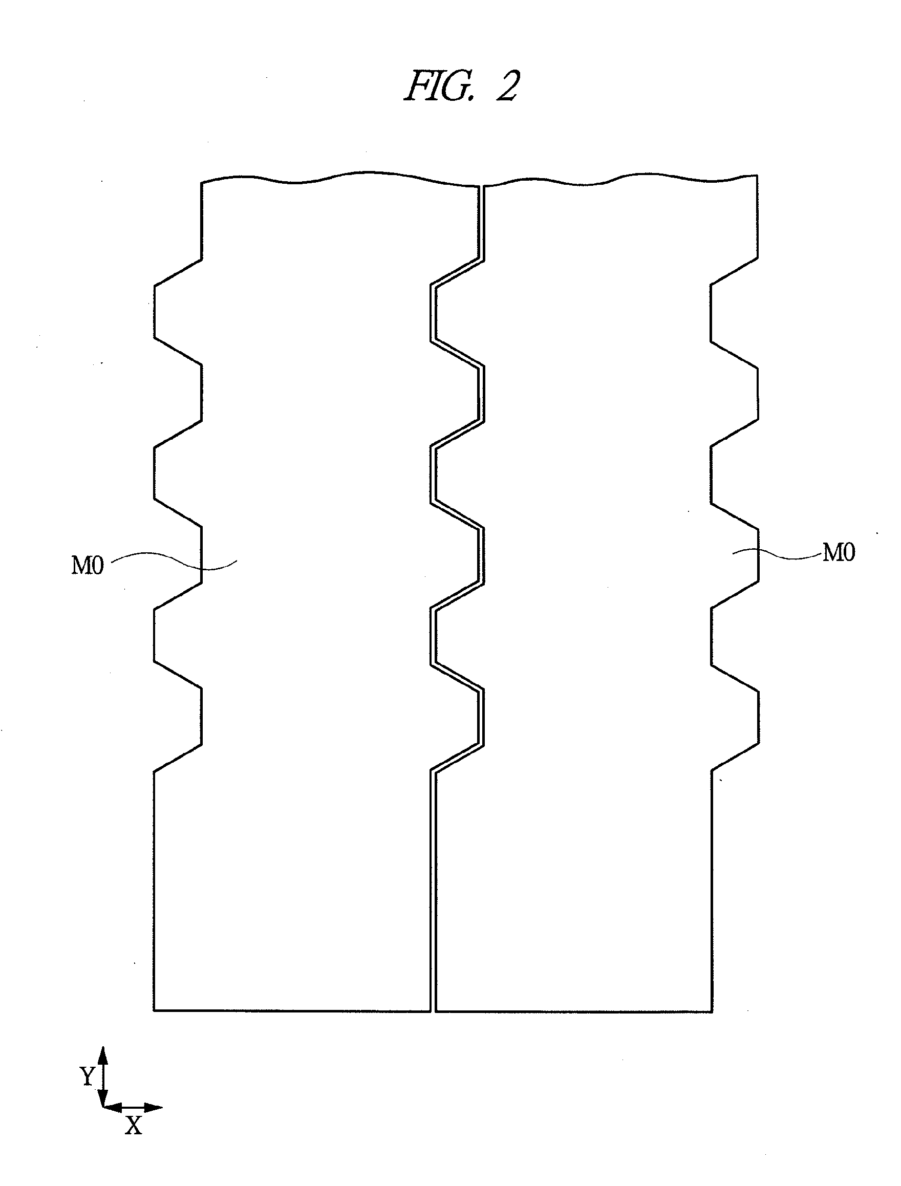
[0088]As shown in FIG. 1, a plane shape of the semiconductor chip 1 is formed in a rectangular shape, for example. A length of the semiconductor chip 1 in a longitudinal direction (second direction Y) is approximately 4 cm, for example, and a length of the semiconductor chip 1 in a short-side dire...
second embodiment
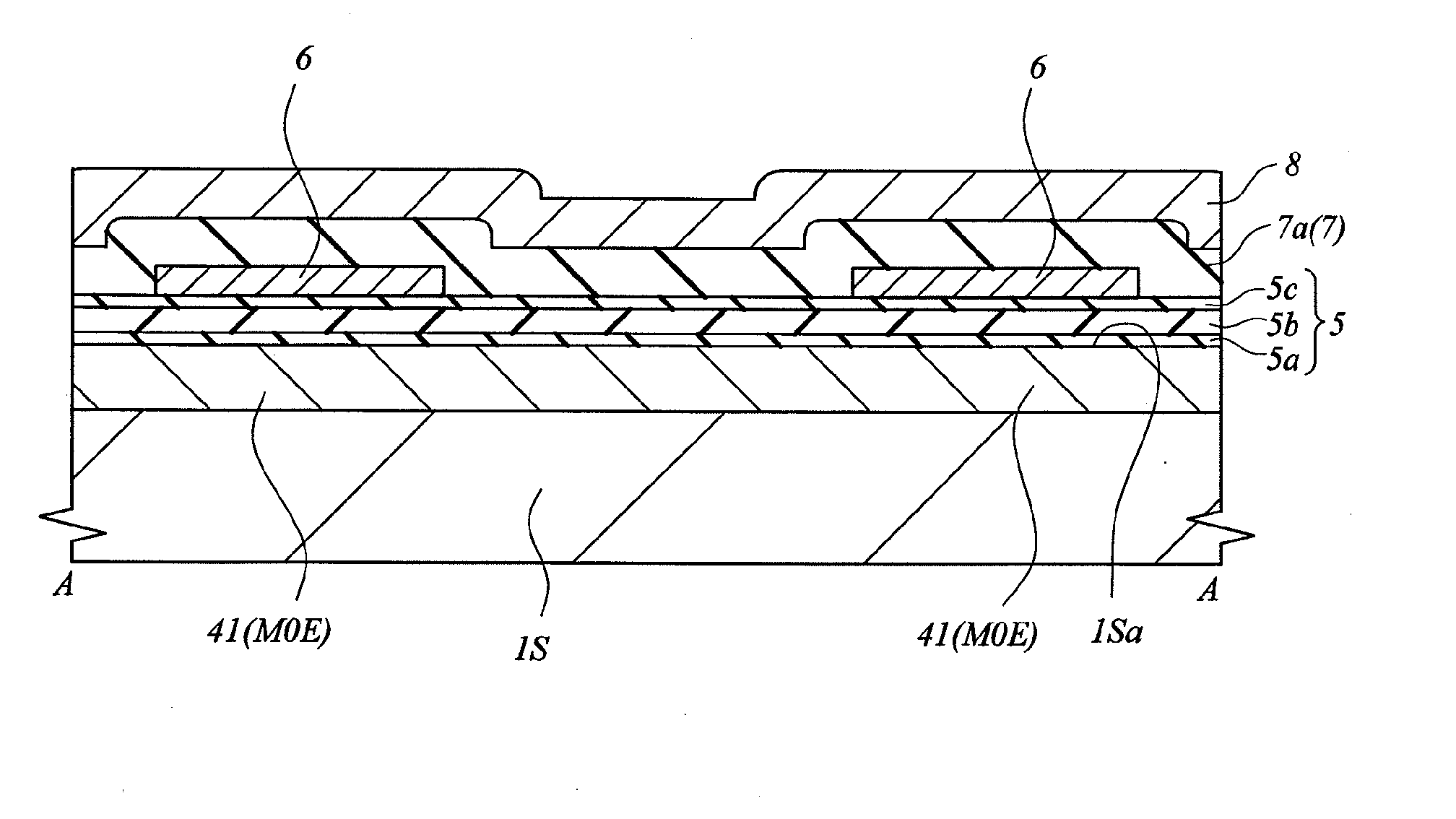
[0168]FIGS. 25 and 26 are main portion cross-sectional views of a semiconductor device according to the present embodiment, and correspond to FIGS. 5 and 6 according to the first embodiment respectively.
[0169]In the first embodiment, as in FIGS. 5 and 6, the insulator film 5 is composed of a stacked film of the silicon oxide film 5a, the silicon nitride film 5b and the silicon oxide film 5c, and the insulator film 7 is composed of a single layer film (single layer) of the silicon oxide film 7a. On the other hand, in the present embodiment, as shown in FIGS. 25 and 26, although the insulator film 5 is composed of a stacked film of the silicon oxide film 5a, the silicon nitride film 5b and the silicon oxide film 5c in the same way as the first embodiment, the insulator film 7 is composed of, unlike the first embodiment, a stacked film of a silicon nitride film 7b and a silicon oxide film 7c sequentially stacked from below (a side of the insulator film 5). Other than that, a configurat...
third embodiment
[0179]FIGS. 28 and 29 are main portion cross-sectional views of a semiconductor device according to the present embodiment, and correspond to FIGS. 5 and 6 of the first embodiment, respectively.
[0180]In the first embodiment, as shown in FIGS. 5 and 6, the insulator film 5 is composed of a stacked film of the silicon oxide film 5a, the silicon nitride film 5b and the silicon oxide film 5c, and the insulator film 7 is composed of a single layer film (single layer) of the silicon oxide film 7a. On the other hand, in the present embodiment, as shown in FIGS. 28 and 29, although the insulator film 5 is composed of a stacked film of the silicon oxide film 5a, the silicon nitride film 5b and the silicon oxide film 5c in the same way as the first embodiment, the insulator film 7 is composed of, unlike the first embodiment, a stacked film of a silicon oxide film 7d, a silicon nitride film 7e and a silicon oxide film 7f sequentially stacked from below (a side of the insulator film 5). Other t...
PUM
 Abstract
Description
Claims
Application Information