

Manufacturing method of semiconductor device and semiconductor device
a manufacturing method and semiconductor technology, applied in the direction of semiconductor devices, electrical devices, transistors, etc., can solve the problems of poor heat stability, low effective work function of materials suitable for the gate electrode of n-channel type misfet, and difficult handling, so as to increase the number of manufacturing processes of semiconductor devices, increase the cost of manufacturing a semiconductor device, and increase the number of manufacturing processes.
- Summary
- Abstract
- Description
- Claims
- Application Information
AI Technical Summary
Benefits of technology
Problems solved by technology
Method used
Image

Examples
first embodiment
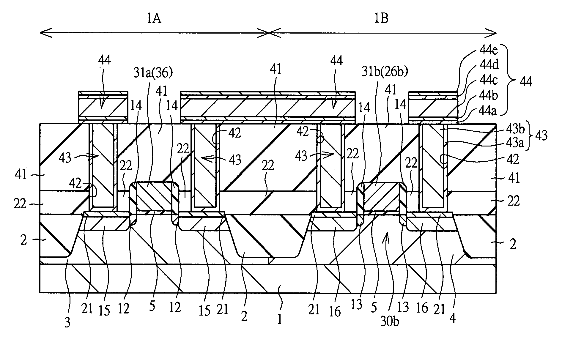
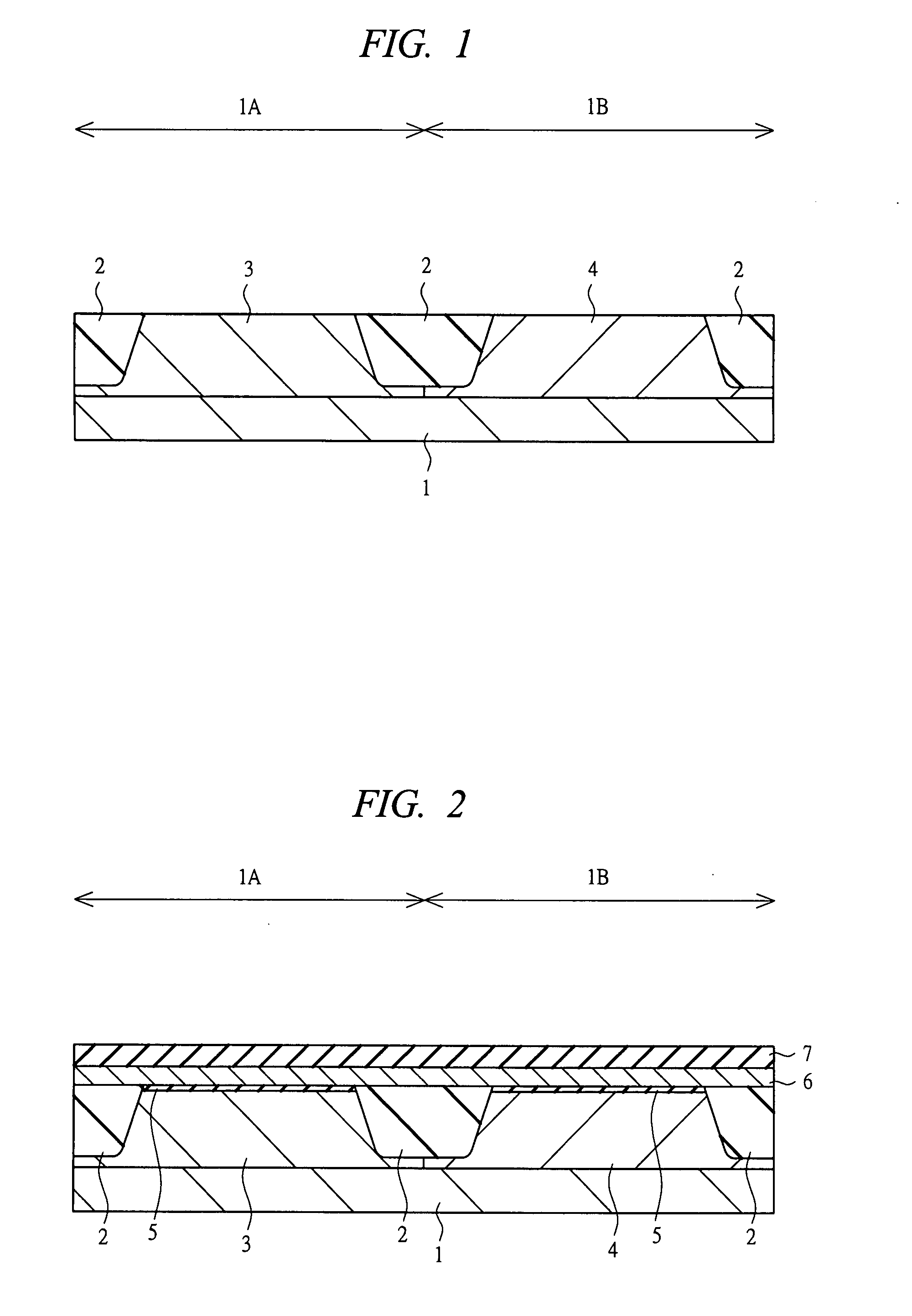
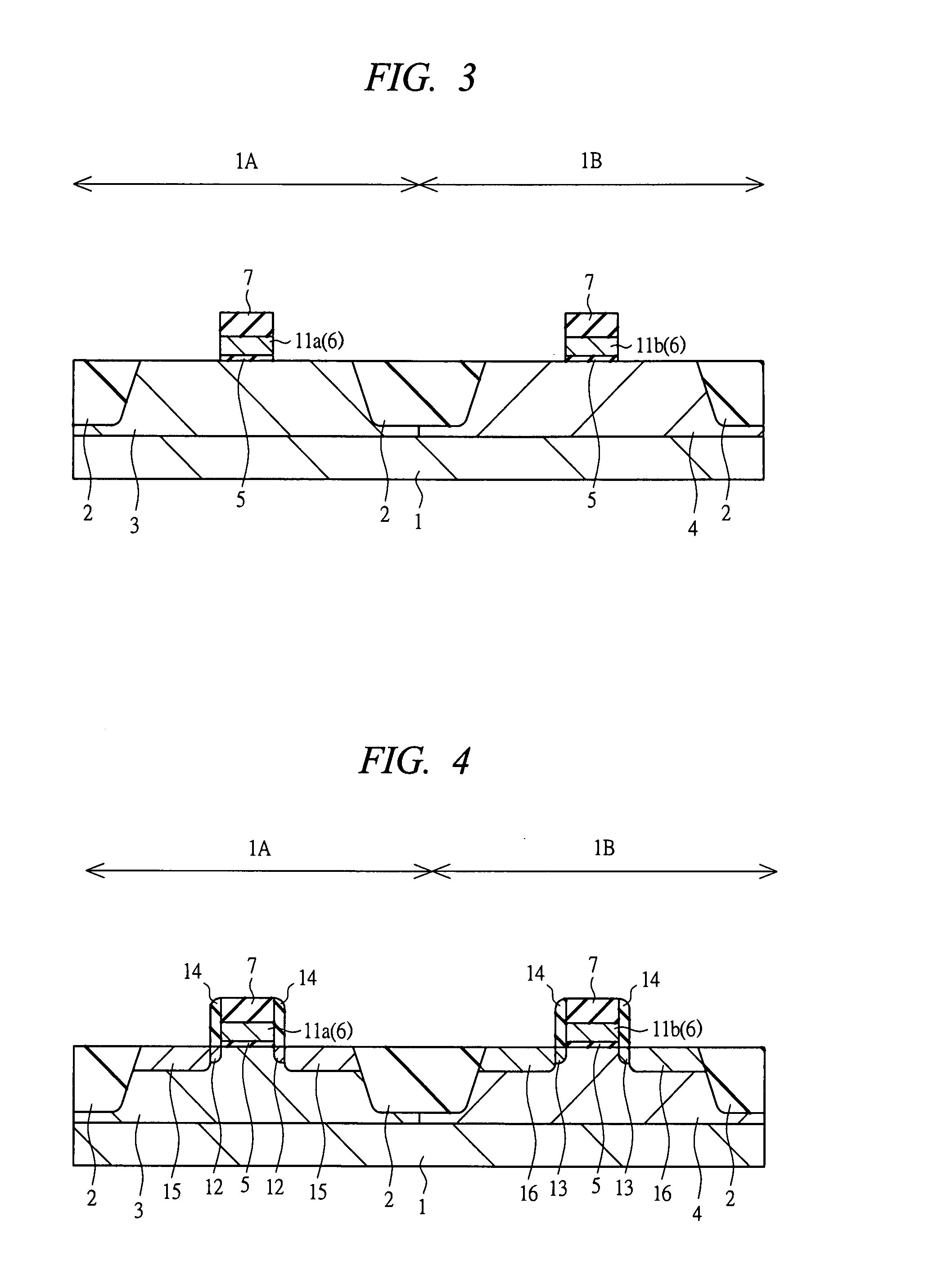
[0043]A semiconductor device and a manufacturing process thereof of the present embodiment will be described with reference to accompanying drawings. FIG. 1 to FIG. 13 are cross-sectional views of main parts of a semiconductor device, for example, a CMISFET (Complementary Metal Insulator Semiconductor Field Effect Transistor) in the manufacturing process thereof in one embodiment of the present invention.
[0044]As shown in FIG. 1, a semiconductor substrate (semiconductor wafer) 1 made of p-type single crystal silicon having resistivity of, for example, in a range of about 1 to 10 Ωcm is prepared. The semiconductor substrate 1 on which the semiconductor device on the present embodiment is formed has an n-channel type MISFET (Metal Insulator Semiconductor Field Effect Transistor) formation region 1A where an n-channel type MISFET is formed and a p-channel type MISFET formation region 1B where a p-channel type MISFET is formed. Then, device isolation regions 2 are formed in the main sur...
second embodiment
[0116]FIG. 15 to FIG. 18 are cross-sectional views of main parts of a semiconductor device in manufacturing processes according to another embodiment of the present invention. Since the processes until FIG. 8 are the same as those of the first embodiment, the repetitive description thereof is omitted and a description about the manufacturing processes continued from FIG. 8 is made here.
[0117]Different from the above-described first embodiment, after the structure of FIG. 8 is obtained in the same manner as the above-described first embodiment, as shown in FIG. 15, a metal film 35a made of the same material as the above-described metal film 35 is formed on the entire surface of the main surface of the semiconductor substrate 1 without forming the insulating film 33 (i.e., on the insulating film 22 and the metal silicide films 26a and 26b) in the same manner (e.g., through sputtering). More specifically, the metal film 35a is formed on the semiconductor substrate 1 so as to cover the ...
PUM
| Property | Measurement | Unit |
|---|---|---|
| resistivity | aaaaa | aaaaa |
| thickness | aaaaa | aaaaa |
| thickness | aaaaa | aaaaa |
Abstract
Description
Claims
Application Information