Semiconductor device and manufacturing method of the same

a technology of semiconductor devices and manufacturing methods, applied in the direction of semiconductor devices, basic electric elements, electrical equipment, etc., can solve the problem that metal silicide films cannot be formed on the entire upper surface of gate electrodes, and achieve the effect of improving the performance of semiconductor devices

Inactive Publication Date: 2006-03-16
RENESAS ELECTRONICS CORP
View PDF1 Cites 21 Cited by
  • Summary
  • Abstract
  • Description
  • Claims
  • Application Information

AI Technical Summary

Benefits of technology

[0020] The performance of the semiconductor device can be improved.

Problems solved by technology

Therefore, the metal silicide film cannot be formed on the entire upper surface of the gate electrode.

Method used


Image

  • Semiconductor device and manufacturing method of the same
  • Semiconductor device and manufacturing method of the same
  • Semiconductor device and manufacturing method of the same

Examples


Embodiment Construction

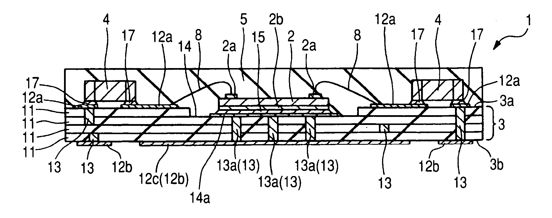
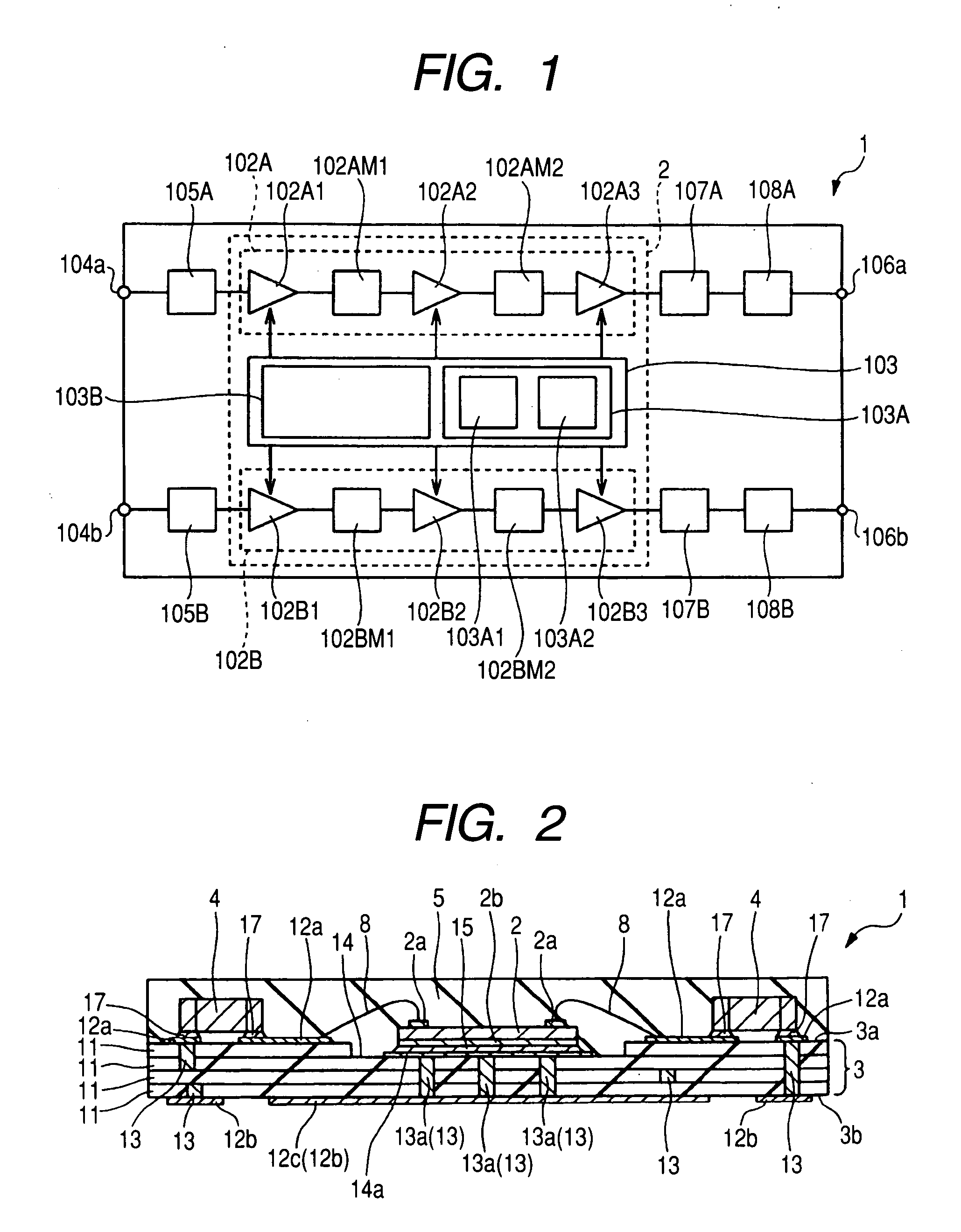
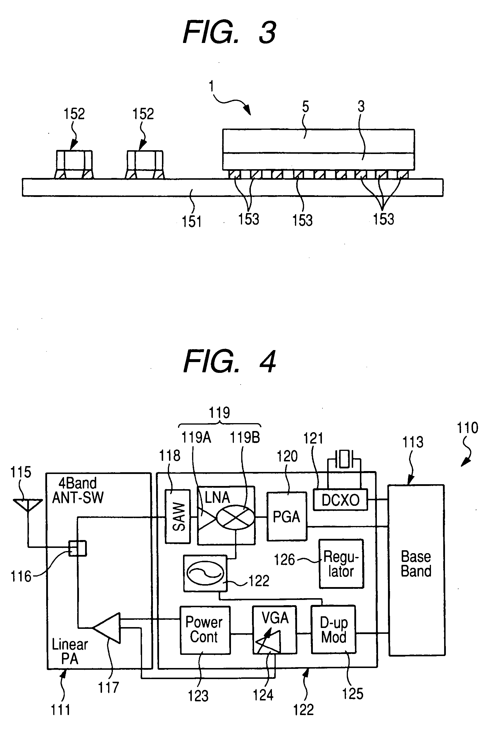
[0056] In the below-described embodiments, for the sake of convenience, the explanation when necessary will be split into a plurality of sections, but unless clearly indicated otherwise, those sections are not unrelated and one of them is related to modification examples, detailed explanation, or auxiliary explanation of all or some of the other sections. Furthermore, in the below-described embodiments, when numbers associated with the elements (including quantities, numerical values, amounts, ranges, and the like) are presented, those specific numbers are not limiting and numbers above and below those specific numbers may be employed, unless clearly indicated otherwise and with the exception of cases where the specific numbers are in principle clearly restrictive. Furthermore, in the below-described embodiments, it goes without saying that constituent elements thereof (including elemental steps and the like) are not always necessary, unless clearly indicated otherwise and with the ...


PUM


Abstract

The invention improves the performance of a semiconductor device. A metal silicide film is formed by a silicide process on a gate electrode and an n+-type source region of an LDMOSFET, and no such metal silicide film is formed on an n−-type offset drain region, an n-type offset drain region, and an n+-type drain region. A side wall spacer comprising a silicon film is formed via an insulating film on the side wall of the gate electrode over the drain side thereof, and a field plate electrode is formed by this side wall spacer. The field plate electrode does not extend above the gate electrode, and a metal silicide film is formed over the entire upper surface of the gate electrode in the silicide process.

Description

CROSS-REFERENCE TO RELATED APPLICATION [0001] The present application claims priority from Japanese patent application No. 2004-263670 filed on Sep. 10, 2004, the content of which is hereby incorporated by reference into this application. BACKGROUND OF THE INVENTION [0002] 1. Field of the Invention [0003] The present invention relates to a semiconductor device and manufacturing method of the same, and more particularly to a technology that can be effectively employed in semiconductor devices used in RF (Radio Frequency) power modules and manufacturing technology of the same. [0004] 2. Description of the Related Art [0005] In recent years, mobile communication devices (the so-called portable phones) represented by communication systems GSM (Global System for Mobile Communications), PCS (Personal Communication Systems), PDC (Personal Digital Cellular) systems, and CDMA (Code Division Multiple Access) systems became popular throughout the world. [0006] Generally, such mobile communicat...

Claims


Application Information

Patent Timeline
Patent Type & Authority Applications(United States)
IPC IPC(8): H01L21/8234H01L21/336
CPCH01L21/823425H01L2224/48227H01L29/0692H01L29/0847H01L29/1045H01L29/402H01L29/66659H01L2924/13091H01L2924/1305H01L21/823468H01L2224/48091H01L2224/32225H01L2924/19105H01L2224/73265H01L2924/00014H01L2924/00H01L2924/181H01L2924/00012
Inventor HATORI, MAKOTOHOSHINO, YUTAKA
Owner RENESAS ELECTRONICS CORP
Why Eureka
Try Eureka