Manufacturing method for metal line

a manufacturing method and metal line technology, applied in semiconductor devices, semiconductor/solid-state device details, electrical apparatus, etc., can solve the problems of damascene copper schemes facing difficulties in manufacturing processes and electrical properties, adversely affecting the filling of metal, and unavoidable high aspect ratio of metal lines, so as to avoid complicated etching processes and accompanying plasma damage, the effect of low parasitic capacitan

Inactive Publication Date: 2014-03-13
NAT APPLIED RES LAB
View PDF1 Cites 18 Cited by
  • Summary
  • Abstract
  • Description
  • Claims
  • Application Information

AI Technical Summary

Benefits of technology

[0021]In summary, by adopting the photolithography process to form the openings for the damascene metal lines, complicated etching processes and the accompanying plasma damage are avoided. Furthermore, by using the electroplating process, electroless plating process or electrophoretic process to grow the metal lines on the first barrier layer at the bottom areas of the openings in a bottom-to-up manner, the height of the metal lines can be controlled to just completely fill the openings. Thus, a chemical mechanical polishing (CMP) process is not required to remove excess metal material. However, it is understood that the chemical mechanical polishing process may be still performed after the metal filling process to control the height of the metal lines or for planarization purpose. According to the present invention, no void occurs within the metal lines.
[0022]In addition, according to the present invention, air gaps are formed in the insulating layer between two adjacent metal lines with smaller spacing. Such structure has low parasitic capacitance and the final device including this metal line structure has an enhanced electrical performance and improved delay.

Problems solved by technology

On the premise of without increasing the device size, higher aspect ratio of metal lines is unavoidable.
With miniaturization of the chips, for example, as device dimensions shrink to a 22 nm node and beyond, damascene copper schemes are facing difficulties in manufacturing processes and electrical properties, especially in controlling defect-free copper gap-filling and retaining reliability such as resistance to electro-migration (EM).
However, the narrow and deep openings with high aspect ratio adversely affect the filling of metal, especially when the diffusion barrier layer and the seed layer cannot be arbitrarily thinned to provide adequate space for the filling In addition, overhang may occur when the seed layer is formed by physical vapor deposition (PVD).
Therefore, the subsequent electroplating process may fail to completely fill the openings and consequentially result in voids within the contacts or wires.
Furthermore, since most metal material has accumulated at upper corners of the insulating layer before the electroplating material reaches the deep bottom during the electroplating process, the vertical growth speed of the metal lines cannot catch up the horizontal narrowing speed of the openings.
Thus, the metal lines may involve internal voids, which lead to a higher resistance and a lower reliability.
However, for the copper lines, the relatively-thin barrier layer may not be able to effectively inhibit copper diffusion.
However, it is difficult to uniformly form a continuous seed layer over the sidewalls of the openings due to limited coverage.
Consequentially, copper may not be deposited on the uncovered portion of the sidewalls in the electroplating process, thereby resulting in the internal voids in the metal lines.
The formation of the high aspect-ratio opening is another challenge.
These disadvantages or problems seriously affect the production yield of the semiconductor devices with scale-down dimension.

Method used


Image

  • Manufacturing method for metal line
  • Manufacturing method for metal line
  • Manufacturing method for metal line

Examples


Embodiment Construction

[0028]The present invention will now be described more specifically with reference to the following embodiments. It is to be noted that the following descriptions of preferred embodiments of this invention are presented herein for purpose of illustration and description only. It is not intended to be exhaustive or to be limited to the precise form disclosed.

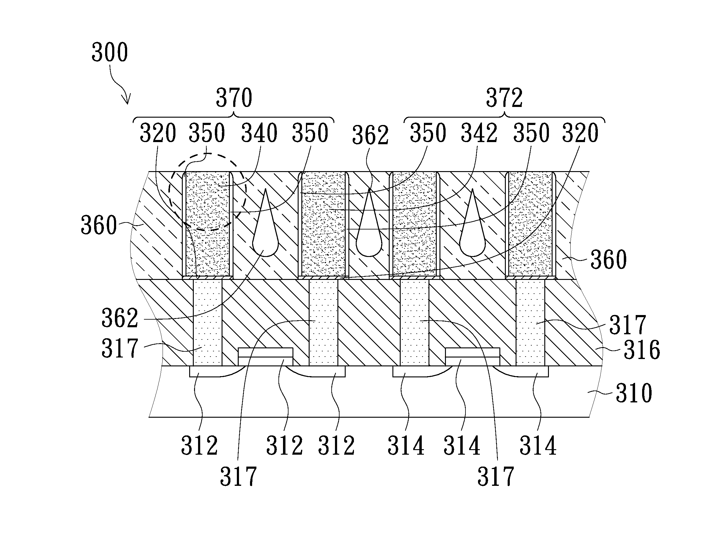
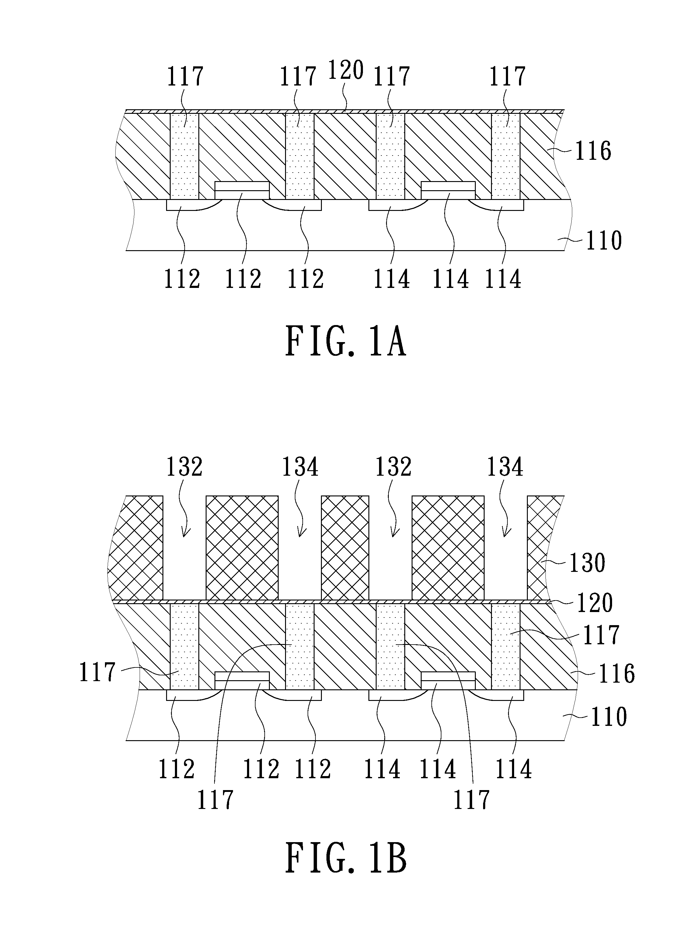
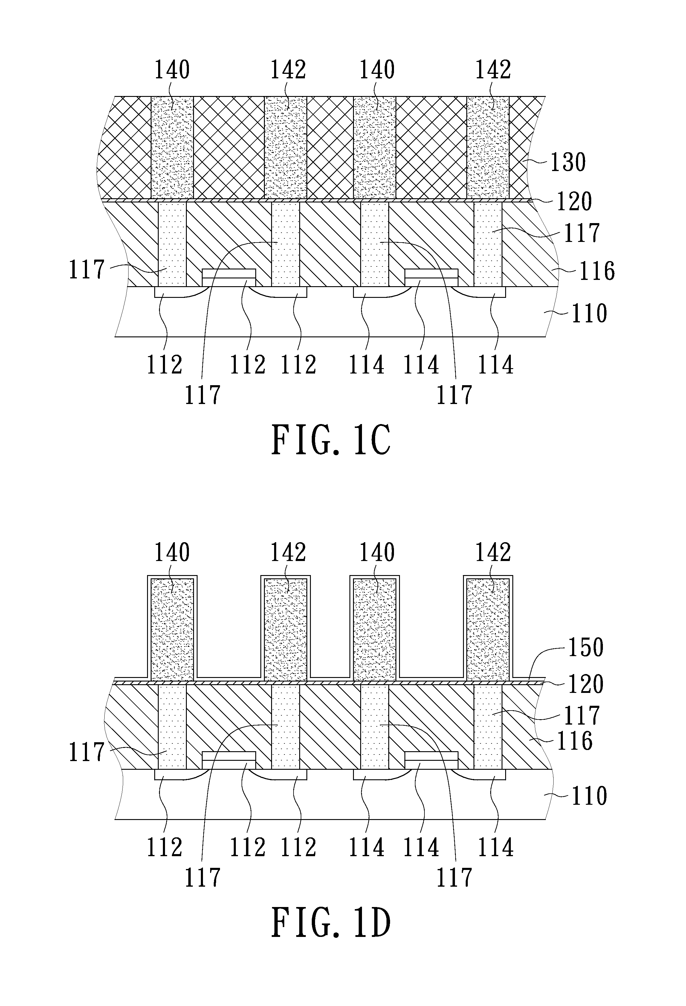
[0029]FIGS. 1A-1F are schematic diagrams illustrating a method for manufacturing metal lines in as semiconductor device in accordance with an embodiment of the present invention. As shown in FIG. 1A, a substrate 110 is provided and a first barrier layer 120 is formed on the substrate 110. Specifically, the first barrier layer 120 is formed by atomic layer deposition (ALD).

[0030]The substrate 110 is a semiconductor substrate (e.g. a silicon substrate) or a metal substrate and has been formed with transistor structures 112, 114, memory structures (not shown) or other circuit elements (not shown). These circuit elements are isolated...


PUM

PropertyMeasurementUnit
areaaaaaaaaaaa
insulatingaaaaaaaaaa
aspect ratioaaaaaaaaaa

Abstract

A method for manufacturing metal lines in a semiconductor device is provided. The method includes steps of: providing a substrate; forming a first barrier layer on the substrate; forming a sacrificial layer on the first barrier layer; forming an opening penetrating through the sacrificial layer to expose a portion of the first barrier layer; depositing a metal material on the exposed first barrier layer to form a metal line in the opening; removing the sacrificial layer and forming a second barrier layer over the resulting structure; etching the second barrier layer and the first barrier layer while remaining a barrier spacer on a sidewall of the metal line; and forming an insulating layer on the substrate and the barrier spacer. A semiconductor device having the metal lines produced by the method is also provided.

Description

CROSS-REFERENCE TO RELATED APPLICATIONS[0001]This application is a Continuation in part of U.S. patent application Ser. No. 13 / 541672, filed on Jul. 4, 2012, now pending. The entirety of the above-mentioned patent application is hereby incorporated by reference herein and made a part of this specification.FIELD OF THE INVENTION[0002]The present invention relates to a method for manufacturing metal lines and a semiconductor device having the metal lines, and more particularly to a method for manufacturing metal lines having high aspect ratio and a semiconductor device having metal lines produced by the same.BACKGROUND OF THE INVENTION[0003]With modern develop of computing hardware, the required transistor density of chips rapidly increases and the corresponding line-width and dimension of semiconductor devices gradually decreases. On the premise of without increasing the device size, higher aspect ratio of metal lines is unavoidable. With miniaturization of the chips, for example, as...

Claims


Application Information

Patent Timeline
Patent Type & Authority Applications(United States)
IPC IPC(8): H01L21/768
CPCH01L21/76841H01L23/53223H01L23/53238H01L23/53252H01L23/53266H01L23/5222H01L23/53295H01L2924/0002H01L21/76885H01L21/7682H01L21/76834H01L21/76852H01L21/76856H01L21/76861H01L21/76867H01L2924/00H01L21/768
Inventor JONG, CHAO-AN
Owner NAT APPLIED RES LAB
Why Eureka
Try Eureka