Nanomagnetically shielded substrate

a shielding substrate and nanotechnology, applied in the field of nanotechnology shielding substrates, can solve the problems of large current flows, large heat generation, and exposed to external sources of severe electromagnetic nois

Inactive Publication Date: 2005-03-08
BIOPHAN TECH
View PDF7 Cites 124 Cited by
  • Summary
  • Abstract
  • Description
  • Claims
  • Application Information

AI Technical Summary

Problems solved by technology

The large current flows so induced often create substantial amounts of heat.
Because living organisms can generally only survive within a relatively narrow range of temperatures, these large current flows are dangerous.
Because the sensing systems and conductive elements of these implantable devices are responsive to changes in local electromagnetic fields, they are vulnerable to external sources of severe electromagnetic noise, and in particular to electromagnetic fields emitted during magnetic resonance imaging (MRI) procedures.
One additional problem with conductors implanted within a living biological organism is that, when they are conducting electricity and are simultaneously subjected to large magnetic fields, a Lorentz force is created which often causes the conductor to move.
This movement may damage body tissue.
Furthermore, the MRI procedures often induce a voltage within the living biological organism.
As little as 0.4 volts is often sufficient to excite muscle (and other) cells and cause them to involuntarily move and / or react, a consequence which is often undesirable.

Method used


Image

  • Nanomagnetically shielded substrate
  • Nanomagnetically shielded substrate
  • Nanomagnetically shielded substrate

Examples


Embodiment Construction

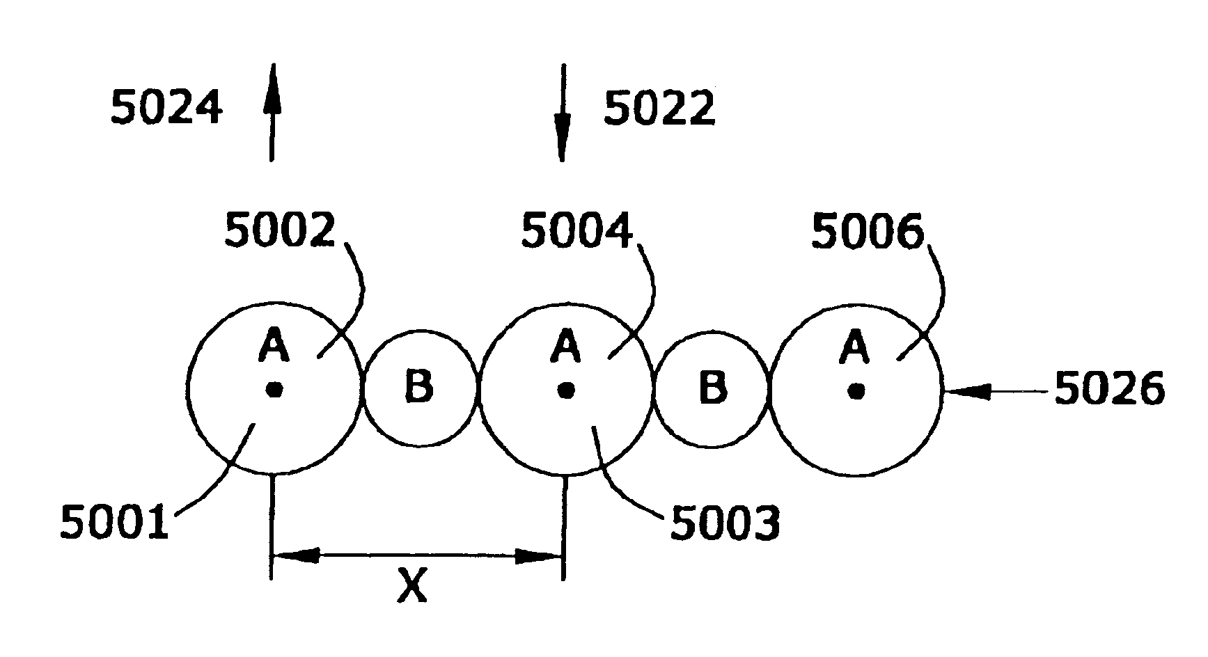
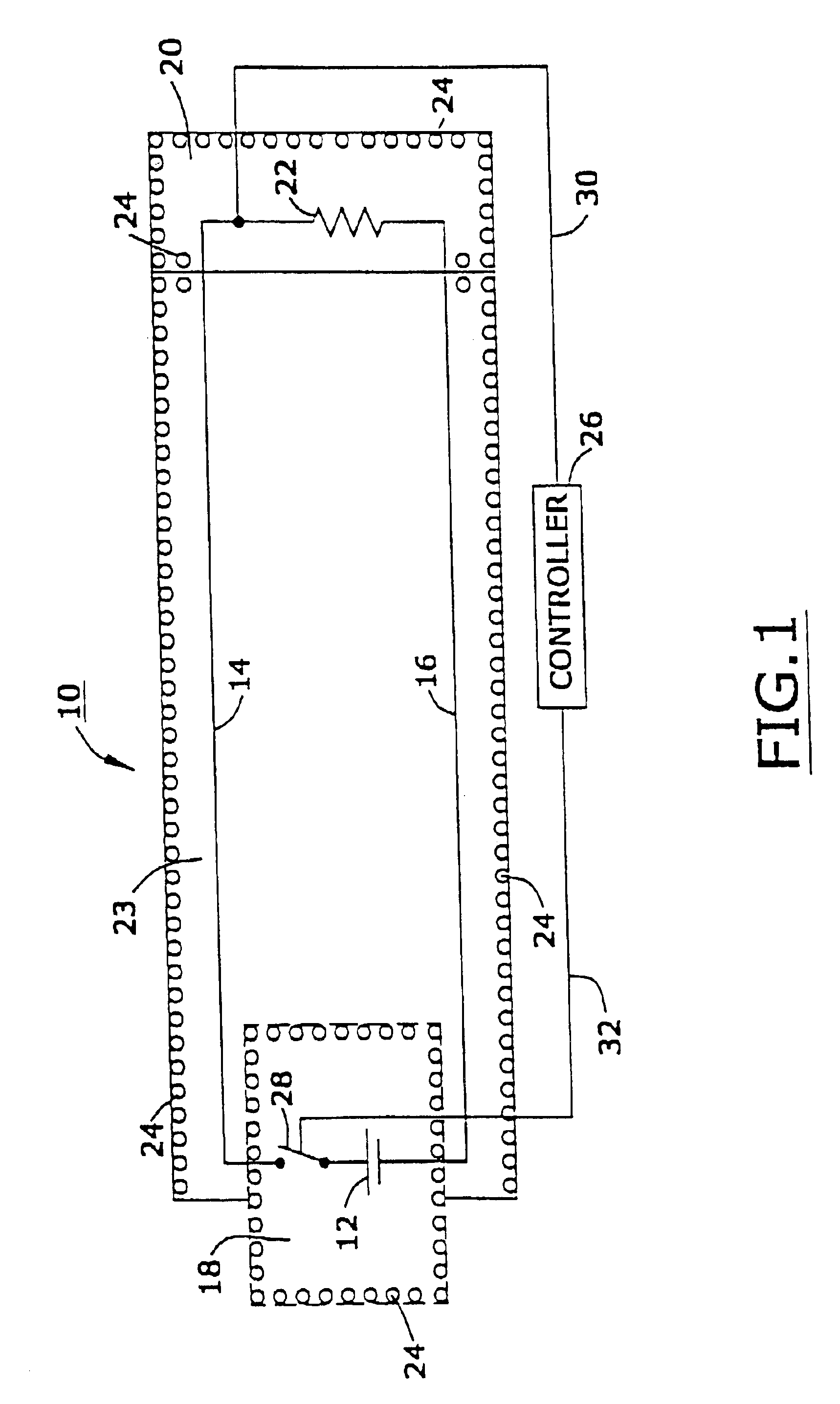
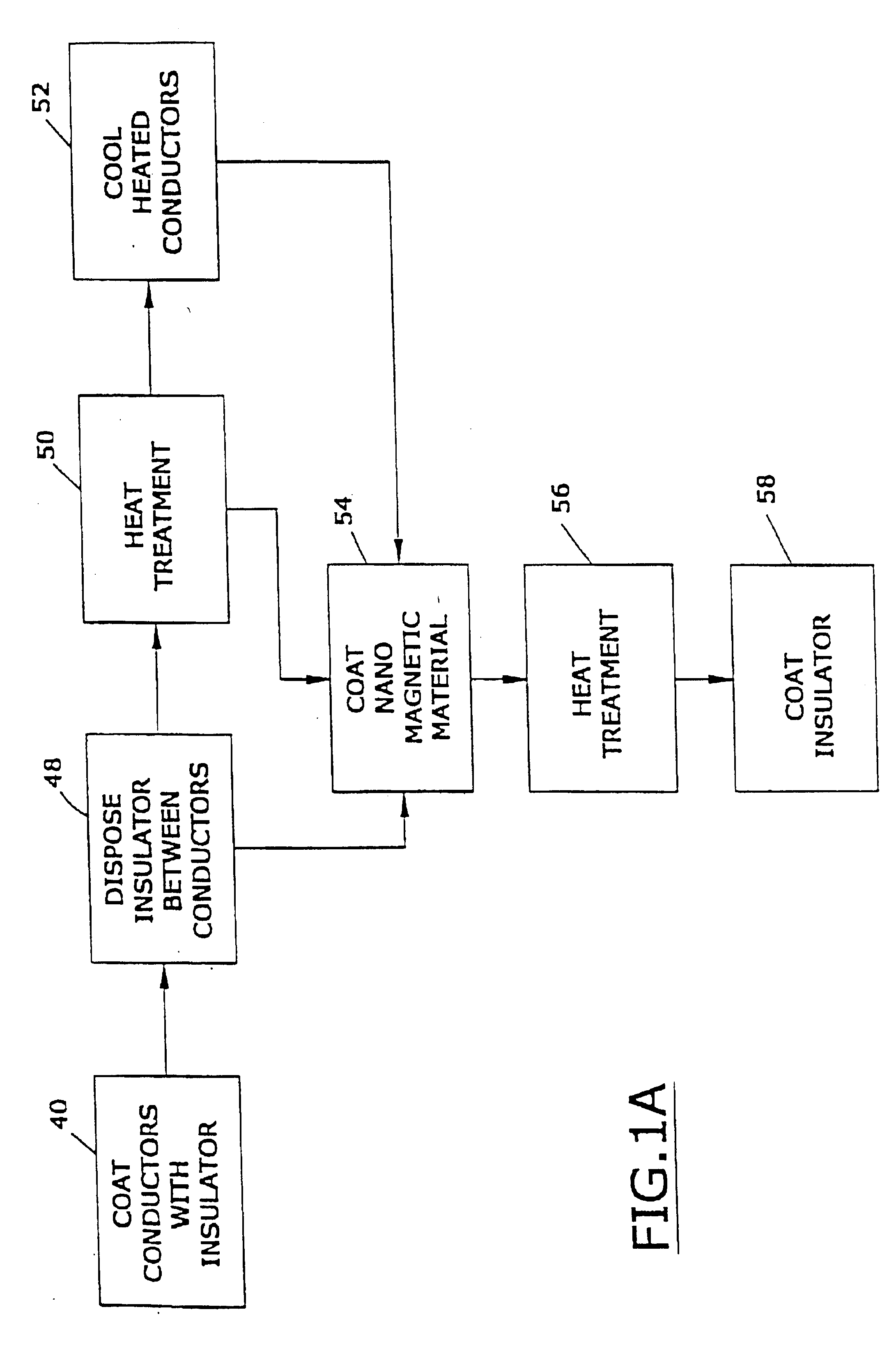
FIG. 1 is a schematic sectional view of one preferred device 10 that, in one embodiment, is implanted in a living biological organism. Referring to FIG. 1, it will be seen that device 10 is comprised of a power source 12, a first conductor 14, a second conductor 16, a first insulative shield 18 disposed about power source 12, a second insulative shield 20 disposed about a load 22, a third insulative shield 23 disposed about a first conductor 14, and a second conductor 16, and a multiplicity of nanomagentic particles 24 disposed on said first insulative shield, said second insulative shield, and said third insulative shield.

In one embodiment, the device 10 is a an implantable device used to monitor and maintain at least one physiologic function, which is capable of operating in the presence of damaging electromagnetic interference; see, e.g., United States published patent application U.S. 20020038135, the entire disclosure of which is hereby incorporated by reference into this speci...


PUM

PropertyMeasurementUnit
magnetic fieldaaaaaaaaaa
particle sizeaaaaaaaaaa
mass densityaaaaaaaaaa

Abstract

A shielded substrate assembly that contains a magnetic shield with a layer of magnetic shielding material; the magnetic shield has a magnetic shielding factor of at least about 0.5. The magnetic shield contains nanomagnetic material nanomagnetic material with a mass density of at least about 0.01 grams per cubic centimeter, a saturation magnetization of from about 1 to about 36,000 Gauss, a coercive force of from about 0.01 to about 5,000 Oersteds, a relative magnetic permeability of from about 1 to about 500,000, and an average particle size of less than about 100 nanometers. The nanomagnetic material contains magnetic material with a coherence length of from about 0.1 to about 100 nanometers.

Description

FIELD OF THE INVENTIONA nanomagnetically shielded substrate comprised of nanomagnetic particles.BACKGROUND OF THE INVENTIONMany implanted medical devices that are powered by electrical energy have been developed. Some of these devices comprise a power source, one or more conductors, and a load. Others of these implantable medical device are passive, with no active energy source.When a patient with one of these implanted devices is subjected to high intensity magnetic fields, on the order of at least about 1 Tesla, currents are often induced in the implanted conductors. The large current flows so induced often create substantial amounts of heat. Because living organisms can generally only survive within a relatively narrow range of temperatures, these large current flows are dangerous.Furthermore, implantable devices, such as implantable pulse generators (IPGs) and cardioverter / defibrillator / pacemaker (CDPs), are sensitive to a variety of forms of electromagnetic interference (EMI). ...

Claims


Application Information

Patent Timeline
Patent Type & Authority Patents(United States)
IPC IPC(8): A61N1/00A61N1/16H01B11/10H01F10/00H01F10/32H01B11/02H01B7/04
CPCA61N1/16B82Y25/00H01B11/10H01F10/007H01F1/0063H01F10/324Y10T428/2982Y10T428/25Y10T428/27Y10T428/24992
Inventor WANG, XINGWUGREENWALD, HOWARD J.
Owner BIOPHAN TECH
Why Eureka
Try Eureka