Liquid crystal display module and scanning circuit board thereof

a liquid crystal display and scanning circuit board technology, applied in the field of scanning technique of liquid crystal display panels, can solve the problems of increasing the delaying problem of scanning lines, worsening the phenomenon of lcd modules with larger sizes and higher resolutions, and improving the quality of lcd modules, so as to reduce the delay effect of each scanning lin

Inactive Publication Date: 2005-12-08
INNOLUX CORP
View PDF6 Cites 12 Cited by
  • Summary
  • Abstract
  • Description
  • Claims
  • Application Information

AI Technical Summary

Benefits of technology

[0012] Therefore, the object of the present invention is to provide an LCD module with identical scanning circuit boards located at both sides of the LCD panel and the connected scan driver ICs would carry out the scanning of each scanning line from both ends, thereby equivalently reducing the delay effect of each scanning line caused by the RC time constant. Accordingly, the quality of the LCD module is improved.
[0013] The present invention achieves the above-indicated objects by providing an LCD module comprising an LCD panel, a driving circuit unit, a first scanning circuit board, a second scanning circuit board, a plurality of first scan driver IC and a plurality of second scan driver IC. The LCD panel has a plurality of scanning lines parallel to its width side. The driving circuit unit is applied to emit a first scanning control signal and a second scanning control signal which are then sent to the first scanning circuit board and the second scanning circuit board, respectively. The first scanning circuit board is configured at the first height side of the LCD panel. The second scanning circuit board is placed at the second height side of the LCD panel. In addition, the first scanning circuit board and the second scanning circuit board have the same circuit layout, and both are provided with a first connector, a second connector and a scanning interface, respectively. The scanning circuit board receives the first scanning control signal via its first connector and sends it to its scanning interface. The second scanning circuit board receives the second scanning control signal via its second connector and sends it to its scanning interface. The first scan driver ICs are coupled between the scanning interface of the first scanning circuit board and a side of the LCD panel to scan the scanning lines sequentially according to the first scanning control signal. Meanwhile, the second scan driver ICs are coupled between the scanning interface of the second scanning circuit board and an opposite side of the LCD panel to scan the scanning lines sequentially according to the second scanning control signal. In addition, the first scan driver ICs and the second scan driver ICs drive the same scanning line synchronously, thereby equivalently reducing the delay effect resulted from the RC time constant.
[0015] Furthermore, the present invention provides a scanning circuit board located in an LCD module with an LCD panel, which comprises a first connector configured at one end of the scanning circuit board for receiving the first scanning control signal, a second connector configured at the other end of the scanning circuit board for receiving the second scanning control signal, and a scanning interface placed at the side of the scanning circuit board for connecting with the scan driver ICs. It is noticed that, in a certain configuration, each scanning circuit board only uses one of the both connectors. When the scanning circuit board is configured at the first height side of the LCD panel and receives the first scanning control signal through the first connector, the scan driver ICs on the scanning interface can scan every scanning line sequentially from the first height side of the LCD panel. In addition, when the scanning circuit board is placed at the second height side of the LCD panel and receives the second scanning control signal from the second connector, the scan driver ICs on the scanning interface can scan every scanning line sequentially from the second height side.

Problems solved by technology

The phenomenon is going to get worse in the LCD modules with larger sizes and higher resolutions.
Hence, when the size and resolution of an LCD get bigger, the delaying problem of the scanning line is getting more serious.
This is the problem encountered when proceeding the driving of a conventional LCD module.

Method used


Image

  • Liquid crystal display module and scanning circuit board thereof
  • Liquid crystal display module and scanning circuit board thereof
  • Liquid crystal display module and scanning circuit board thereof

Examples


Embodiment Construction

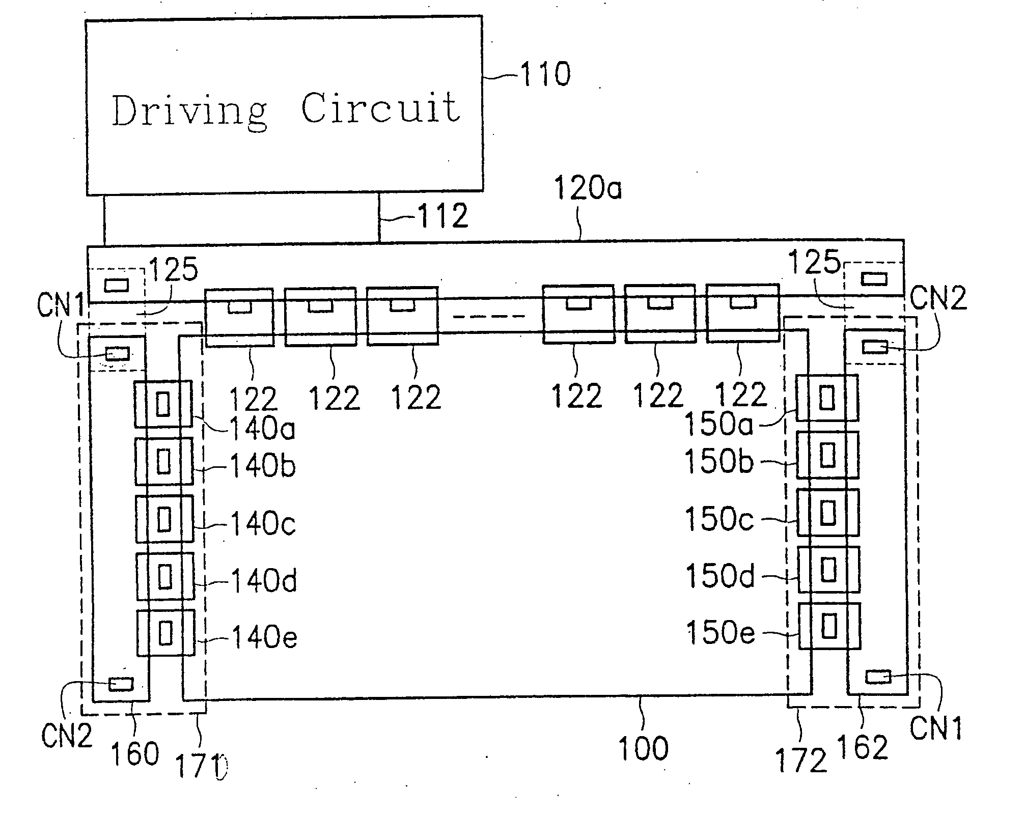
[0023] The present invention is to provide a solution to the delay effect caused by RC time constant of the scanning lines in driving the LCD panel. The present invention can be applied to the LCD with bigger sizes and higher resolutions developed in the future. The embodiment of the present invention is to provide identical scan driver ICs at the both sides of the LCD panel respectively (namely the two ends of each scanning line) and to scan one of the scanning lines from the both ends at the same time, thereby equivalently reducing the equivalent RC time constant. Because the scanning operation is performed from both ends of each scanning line, the greatest delay would occur at the center of the picture frame.

[0024] To realize the scanning method described, the embodiment of the present invention uses identical scan driver ICs and scanning circuit boards to implement the driving mechanism at the both ends of the scanning lines, thereby reducing the number of the components requir...


PUM


Abstract

A liquid crystal display module and its scanning circuit board therein. There are a first scanning circuit and a second scanning circuit located at both ends of each of the scanning lines in the LCD panel. While scanning, both the first scanning circuit and the second scanning circuit drive the same scanning line simultaneously, so as to equivalently reduce the delay effect caused by the RC time constant. The first scan driving circuit and the second scan driving circuit could be placed on different scanning circuit boards with the same layout. The scanning circuit board has two connectors at the both ends and a scanning interface at a side. The scanning circuit board could be used at both sides of the LCD panel by the rotation of 180°.

Description

[0001] This is a continuation of co-pending U.S. patent application Ser. No. 09 / 609651, filed Jul. 3, 2000.BACKGROUND OF THE INVENTION [0002] 1. Field of the Invention [0003] The present invention relates to a scanning technique of an LCD (liquid crystal display) panel. More particularly, this invention relates to an LCD module with symmetrical scanning circuit boards at the two ends of the LCD panel. [0004] 2. Description of the Related Art [0005]FIG. 1 (Prior Art) is a plane view of a conventional LCD module. As shown in FIG.1, the LCD module comprises an LCD panel 100, a data circuit board 120, a plurality of data driver integrated circuits (ICs) 122, a scanning circuit board 130, a plurality of scan driver ICs 132, and a driving circuit 110. Driving circuit 110 connects to data circuit board 120 via connecting line 112 for transferring corresponding data driving signals and scanning control signals. Data circuit board 120 then connects to scanning circuit board 130 through conne...

Claims


Application Information

Patent Timeline
Patent Type & Authority Applications(United States)
IPC IPC(8): G09G3/18G09G3/36G09G5/00
CPCG09G3/3666G09G2320/0223G09G2310/0283G09G3/3677
Inventor LIN, TIEN-JENWU, BIING-SENG
Owner INNOLUX CORP
Why Eureka
Try Eureka