Liquid Crystal Display Device, Low Temperature Poly-Silicon Display Device, and Manufacturing Method Thereof

a display device and liquid crystal technology, applied in semiconductor devices, instruments, optics, etc., can solve the problems of affecting throughput, requiring an extended period of time to complete the whole process, and high manufacturing cost, so as to reduce the reduce the electrical resistance of the common electrode, and alleviate the delay

Inactive Publication Date: 2013-06-27
SHENZHEN CHINA STAR OPTOELECTRONICS TECH CO LTD
View PDF5 Cites 5 Cited by
  • Summary
  • Abstract
  • Description
  • Claims
  • Application Information

AI Technical Summary

Benefits of technology

[0022]The efficacy of the present invention is that to be distinguished from the state of the art, the present invention realizes reduction of the resistance of the common electrode and alleviation the delay effect caused by excessively large electrical resistance of the common electrode by providing electrical connection of the common electrode to an existing metal shield layer, so that there is no need to specifically form a metal layer that is made in parallel connection with the common electrode in order to reduce the electrical resistance of the common electrode, whereby the number of application of mask is reduced by one and the period of time with which a complete manufacturing process is done can be reduced to lower down the cost and improve the throughput.

Problems solved by technology

Such a manufacturing process is expensive and an extended period of time is required to complete the whole process.
This severely affects the throughput.

Method used


Image

  • Liquid Crystal Display Device, Low Temperature Poly-Silicon Display Device, and Manufacturing Method Thereof
  • Liquid Crystal Display Device, Low Temperature Poly-Silicon Display Device, and Manufacturing Method Thereof
  • Liquid Crystal Display Device, Low Temperature Poly-Silicon Display Device, and Manufacturing Method Thereof

Examples


Embodiment Construction

[0026]A detailed description of a low temperature poly-silicon display device according to an embodiment of the present invention will be given in order to more clearly disclose specifics and spirit of the present invention.

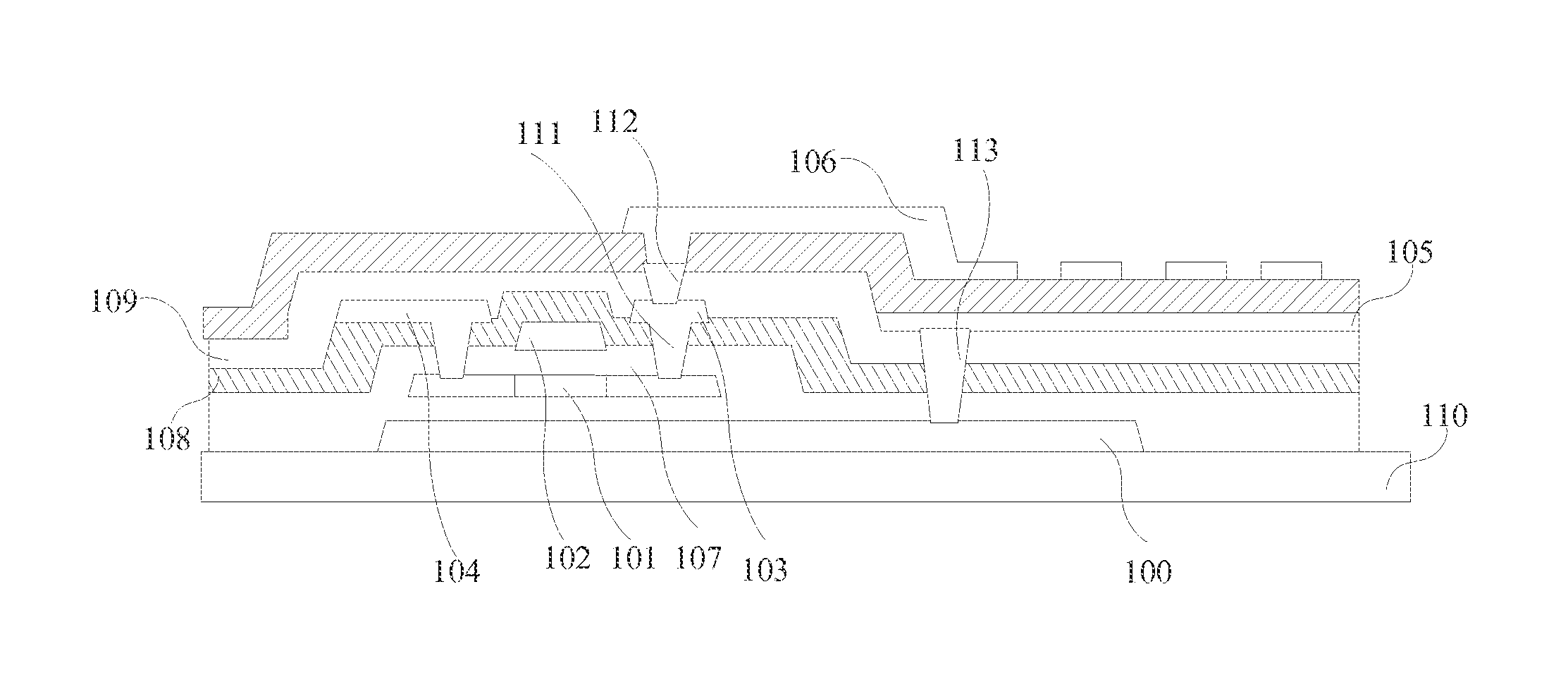
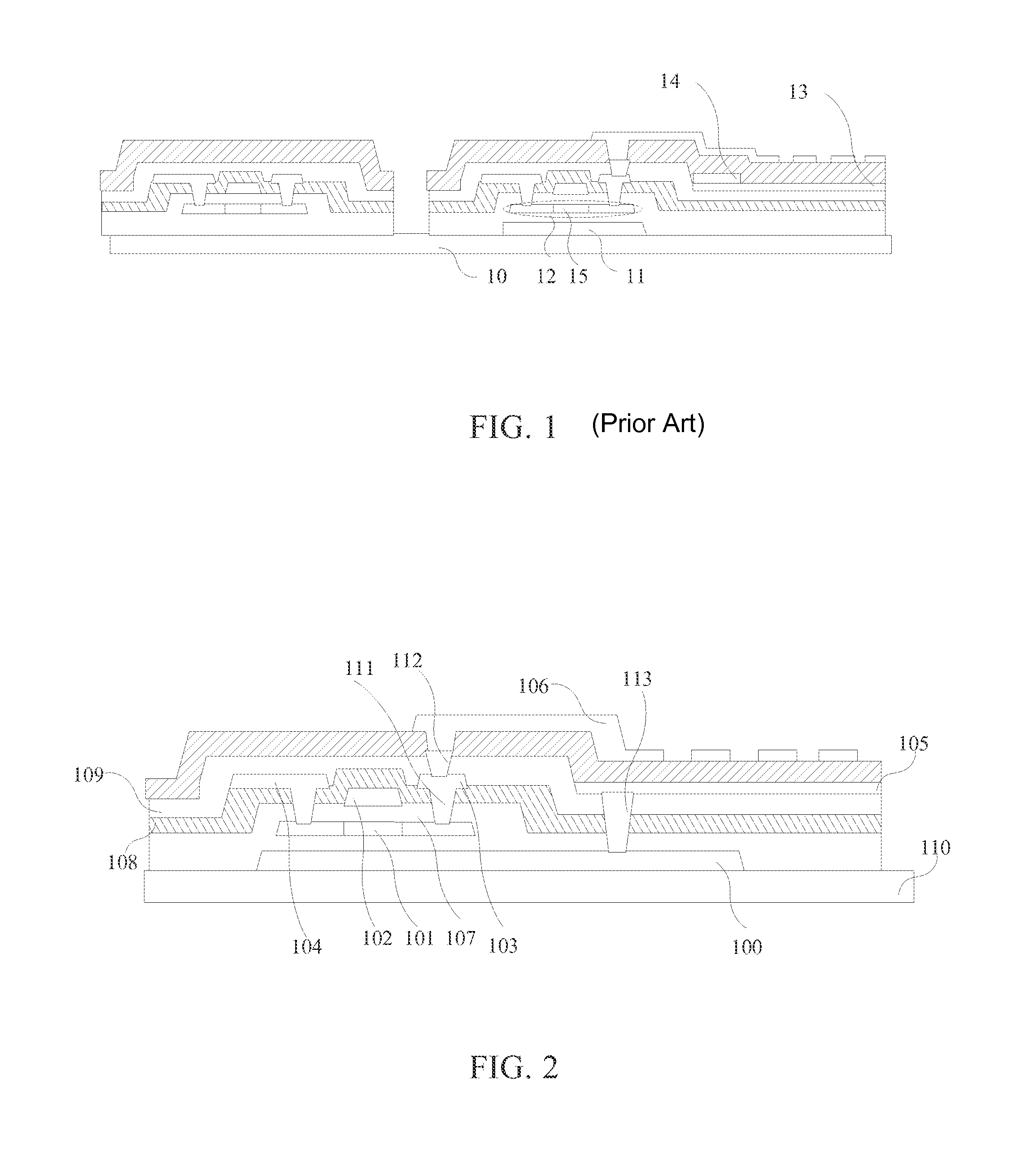
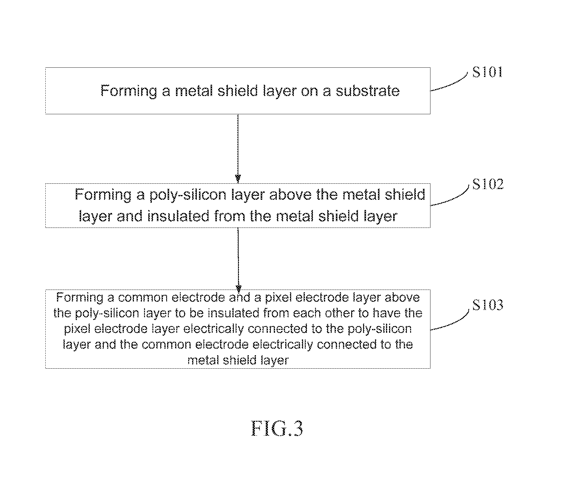
[0027]Referring to FIG. 2, FIG. 2 is a partial cross-sectional view of a thin-film transistor substrate of low temperature poly-silicon display device according to an embodiment of the present invention. The low temperature poly-silicon display device comprises:[0028]a substrate 110, a metal shield layer 100, a poly-silicon layer 101, a gate metal layer 102, a source metal layer 103, a drain metal layer 104, a common electrode 105, and a pixel electrode layer 106.

[0029]The metal shield layer 100 is arranged on the substrate 110 to reduce leakage current caused by light illumination.

[0030]The poly-silicon layer 101 is formed above the metal shield layer 100 and is insulated from the metal shield layer 100. The gate metal layer 102 is arranged above the poly-silico...


PUM

PropertyMeasurementUnit
temperatureaaaaaaaaaa
conductiveaaaaaaaaaa
resistanceaaaaaaaaaa

Abstract

The present invention discloses a liquid crystal display device, a low temperature poly-silicon display device, and a manufacturing method thereof. The manufacturing method includes: forming a metal shield layer on a substrate; forming a poly-silicon layer above the metal shield layer and insulated from the metal shield layer; and forming a common electrode and a pixel electrode layer above the poly-silicon layer to be insulated from each other to have the pixel electrode layer electrically connected to the poly-silicon layer and the common electrode electrically connected to the metal shield layer. Through the above described method, the present invention reduces the resistance of the common electrode, reduces the delay effect caused by excessively large electrical resistance of the common electrode, reduces the number of masking operation by one, reduces the period of time by which a manufacturing process is completed, lowers down the cost, and increases the throughput.

Description

BACKGROUND OF THE INVENTION[0001]1. Field of the Invention[0002]The present invention relates to the field of displaying techniques, and in particular to a liquid crystal display device, a low temperature poly-silicon display device, and a manufacturing method thereof.[0003]2. The Related Arts[0004]Low temperature poly-silicon techniques have been widely applied to liquid crystal display devices and / or organic light-emitting diodes by being used in combination with IPS (In-Plane Switching) or FFS (Fringe Field Switching) techniques to provide improved displaying characteristics and to better meet the needs of general consumers.[0005]As shown in FIG. 1, conventionally, a low temperature poly-silicon display device comprises: a substrate 10, a metal shield layer 11, a poly-silicon layer 12, a common electrode 13, and a metal layer 14. The metal shield layer 11, the poly-silicon layer 12, the common layer 13, and the metal layer 14 are sequentially formed on the substrate 10, in which ...

Claims


Application Information

Patent Timeline
Patent Type & Authority Applications(United States)
IPC IPC(8): G02F1/1343H01L29/16H01L33/02
CPCH01L27/124H01L27/1288G02F2202/104G02F1/13439G02F2001/136231G02F1/134363G02F1/136231
Inventor ZHOU, XIU-FENG
Owner SHENZHEN CHINA STAR OPTOELECTRONICS TECH CO LTD
Why Eureka
Try Eureka