

SRAM employing virtual rail scheme stable against various process-voltage-temperature variations
- Summary
- Abstract
- Description
- Claims
- Application Information
AI Technical Summary
Benefits of technology
Problems solved by technology
Method used
Image

Examples
Embodiment Construction
[0033] The attached drawings for illustrating preferred embodiments of the present invention are referred to in order to gain a sufficient understanding of the present invention, the merits thereof, and the objectives accomplished by the implementation of the present invention.
[0034] Hereinafter, the present invention will be described in detail by explaining preferred embodiments of the invention with reference to the attached drawings. Like reference numerals in the drawings denote like elements.
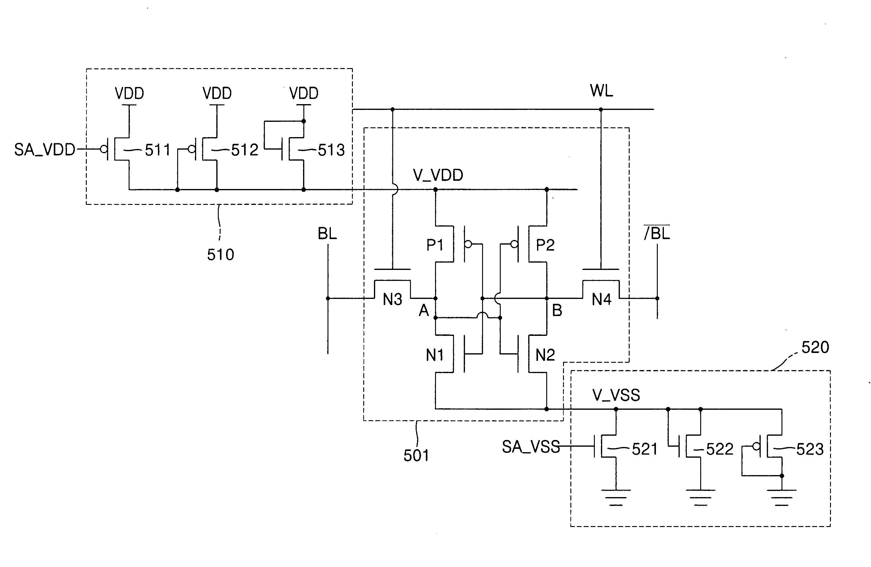
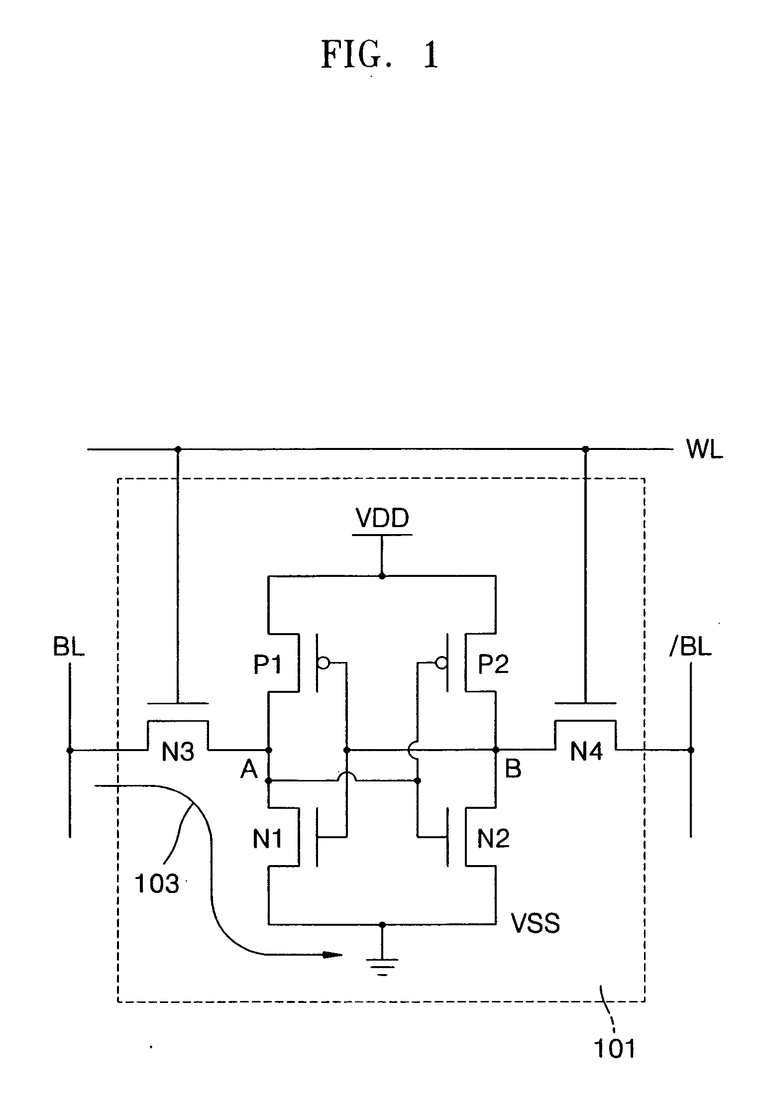
[0035]FIG. 5 illustrates a SRAM having a virtual rail scheme according to an embodiment of the present invention. Referring to FIG. 5, an SRAM cell 501 is configured substantially the same as the SRAM cell 101 of FIG. 1 except that sources of transistors P1 and P2 are not connected to a power supply voltage VDD but rather are connected to a virtual power supply voltage V13 VDD transmitted via a first bias device 510 and that sources of transistors N1 and N2 are not connected to a ground ...
PUM
 Abstract
Description
Claims
Application Information