Flash memory device with a plurality of protocols and a method for controlling the flash memory device
a flash memory device and plurality of protocols technology, applied in the field of flash memory devices, can solve the problems that none of flash memory devices (i.e. flash memory cards) on the market support sd and mmc dual protocols
- Summary
- Abstract
- Description
- Claims
- Application Information
AI Technical Summary
Benefits of technology
Problems solved by technology
Method used
Image
Examples
first embodiment
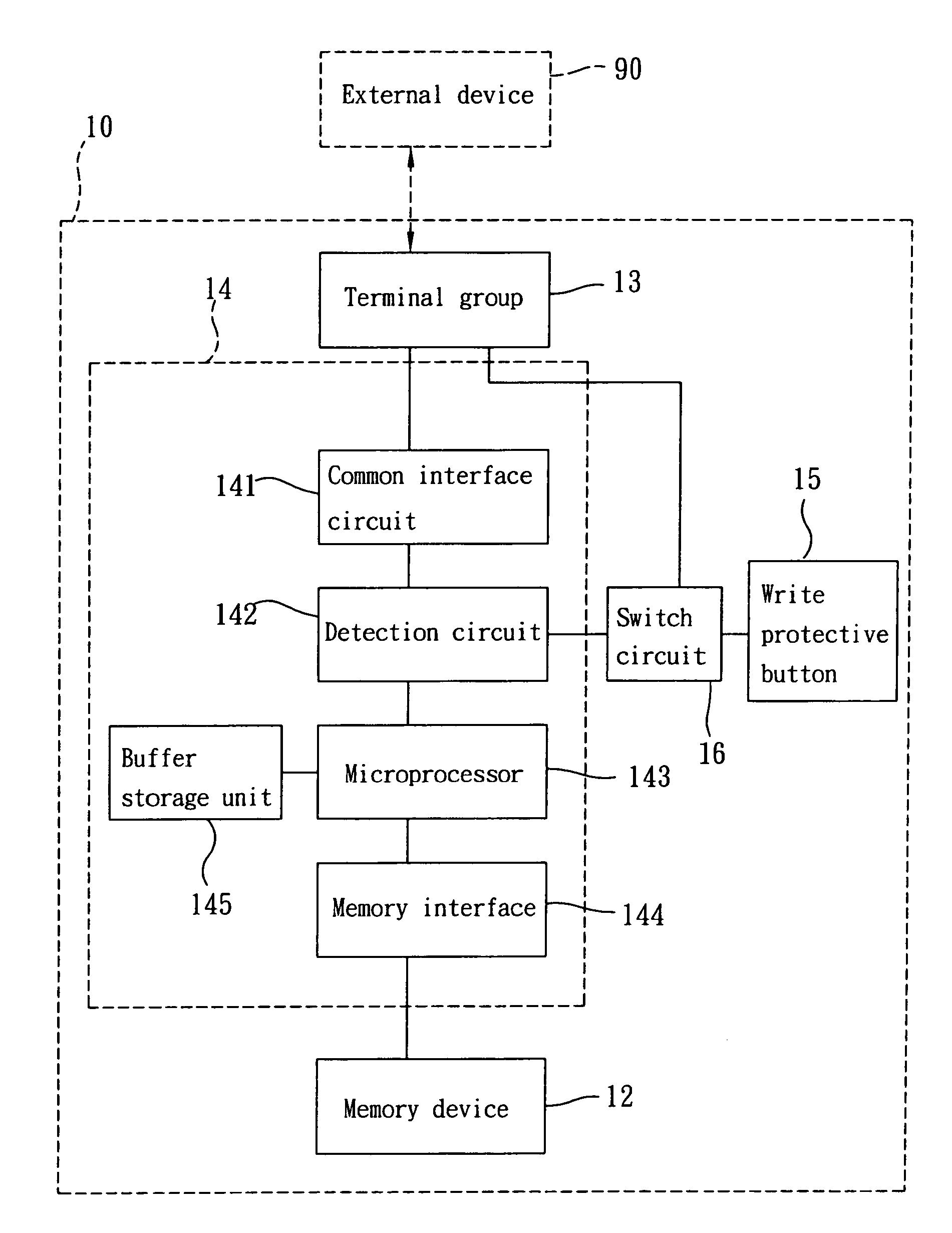
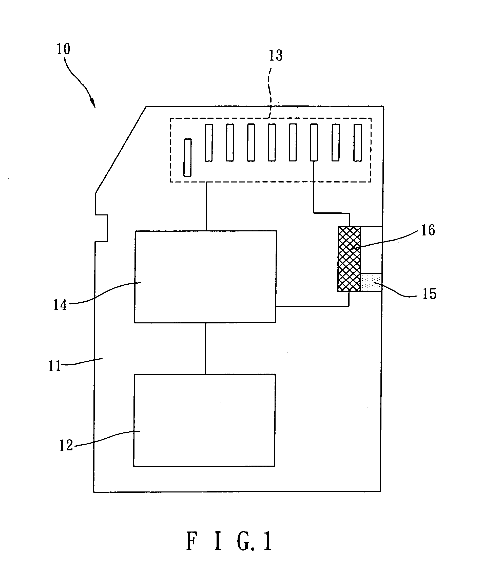
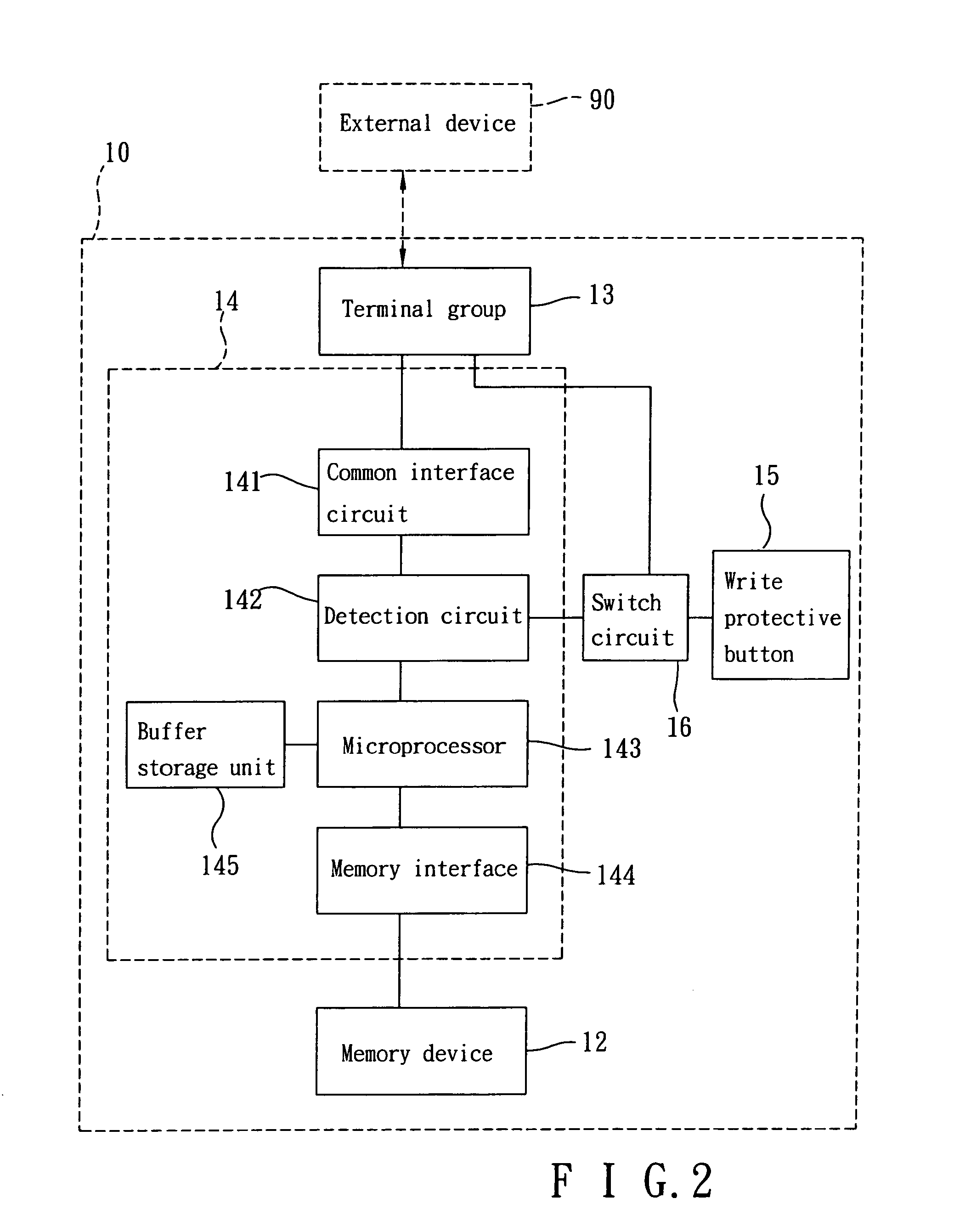
[0025] As shown in FIG. 1 and FIG. 2, the flash memory device 10 with a plurality of protocols according to the invention comprises a body 11, a memory device 12, a terminal group 13, a control unit 14, a write protect button 15, and a switch circuit 16.
[0026] The profile size of the body 11 meets the specification of a Secure Digital card (SD) and hence is compatible with the profile specification of a MultiMedia card (MMC). It is also possible to design the body 11 to make it meet the profile specification of a MultiMedia card (MMC) and that, of course, is still compatible with the profile specification of a Secure Digital card (SD).
[0027] The memory device 12 is mounted on the body 11 and consists of a plurality of rewritable non-volatile memory. In this preferred embodiment, the memory device 12 preferably comprises at lease a flash memory.
[0028] The terminal group 13 is furnished on the front side part of the body 11 and is exposed to the outside. The terminal group 13 may be...
second embodiment
[0053] Referring to FIG. 4, the circuit block diagram of the flash memory device 10a with a plurality of protocols in the invention is shown. The flash memory device 10a shown in FIG. 4 is almost the same as the embodiment shown in FIG. 2 and also comprises a body 11a, a memory device 12a, a terminal group 13a, a control unit 14a, a write protect button 15a, and a switch circuit 16a. The flash memory device 10a is also connectable to an external device 90a. Similarly, the control unit 14a also comprises a detection circuit 142a, a microprocessor 143a, a memory interface 144a, and a buffer storage unit 145a. The only difference is that, the control unit 14a of the flash memory device 10a shown in FIG. 4 is not furnished with a common interface circuit, but is directly coupling the terminal group 13a to appropriate contacts of the detection circuit 142a by conductive wires.
[0054] Referring to FIG. 5, a flowchart of a second preferred embodiment of the control method, i.e. the detectio...
PUM
 Abstract
Description
Claims
Application Information


