

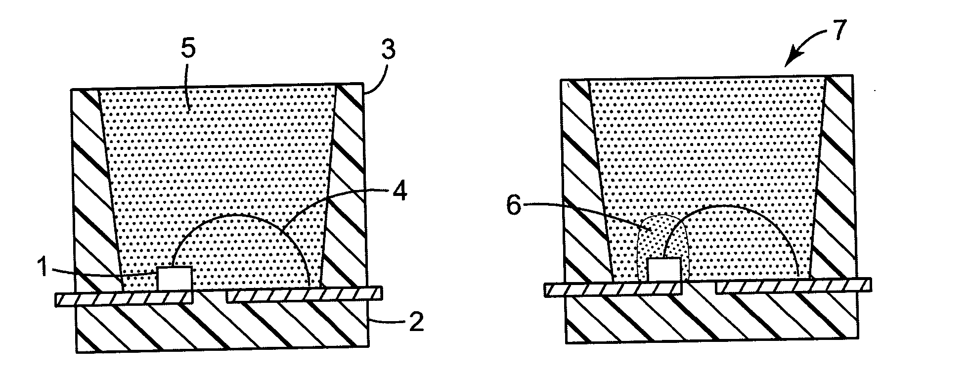
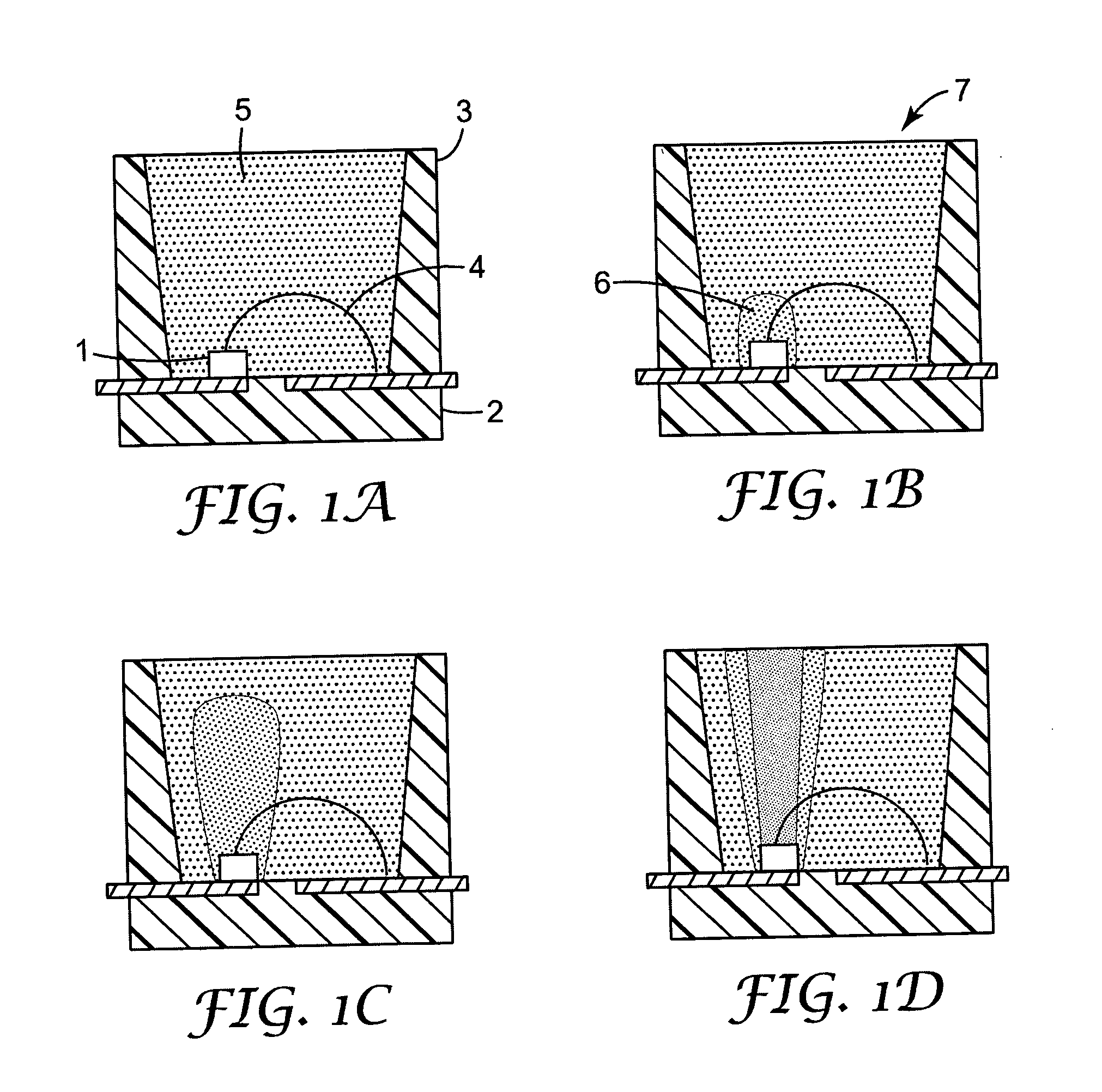
Encapsulated light emitting diodes and methods of making
a light-emitting diode and light-emitting diode technology, applied in the field of encapsulated light-emitting diodes and methods of making, can solve the problems of light loss at the bond site, achieve the effects of reducing or limiting mechanically generated stress, high tensile modulus, and diffuse more easily
- Summary
- Abstract
- Description
- Claims
- Application Information
AI Technical Summary
Benefits of technology
Problems solved by technology
Method used
Image

Examples
example 1
Photobleaching Encapsulant For Green Or Blue LED
[0055] A mixture of 103.80 grams of bisphenol A diglycidylether dimethacrylate, 207.70 grams of PEG40DMA (a polyethyleneglycol-dimethacrylate), 1466.00 grams of a 1:1 mixture of CDMA (a carboxylated dimethacrylate) and PEG400DMA, 41.60 grams of ethyl (4 dimethylamino)benzoate, 9.24 grams of butylated hydroxytoluene, 9.26 grams of camphorquinone, 13.9 grams of diphenyliodonium hexafluorophosphate, and 0.46 grams of Erythrosin yellow blend (90% Erythrosin B and 10% Erythrosin Y) was prepared in a 5 liter round bottom flask. The resin was prepared under yellow light to avoid inadvertent photoreaction and was stored in a brown plastic Nalgene bottle.
example 2
LED Curing Of Photobleachable Encapsulant
[0056] To a blue LED package was added approximately 2 milligrams of low viscosity, pink colored photoreactive methacrylate resin from Example 1. Electrical contact was made to the LED package and 20 milliamperes of current was passed through the LED. The LED was illuminated for approximately 2 minutes. The methacrylate resin encapsulant was completely cured, solid, and clear and light yellow in color with no visible pink color. The cured resin was substantially uniform in refractive index throughout its volume.
example 3
Blue Light Cured Organosiloxane Encapsulant
[0057] A mixture of 10.00 grams (g) of the vinyl siloxane base polymer H2C═CH—Si(CH3)2O—(Si(CH3)2O)100—Si(CH3)2—CH═CH2 (olefin milliequivalent weight (meq wt)=3.801 grams) and 0.44 g of the siloxane crosslinking agent (CH3)3SiO—(Si(CH3)2O)15—(SiH(CH3)O)25—SiMe3 (Dow Coming Syl-Off 7678, Si-H meq wt=0.111 g) was prepared in a 35 milliliter (mL) amber bottle. A catalyst stock solution as prepared by dissolving 22.1 mg of Pt(acac)2 (wherein acac is acetoacetonate, purchased from Aldrich Chemical Company) in 1.00 mL of CH2Cl2, and a 100-microliter (μL) aliquot of this solution was added to the mixture of siloxane polymers. The final formulation was equivalent to a C═C / Si—H functionality ratio of 1.5 and contained approximately 100 ppm of Pt.
PUM
 Abstract
Description
Claims
Application Information