Image sensor with self-boosting and methods of operating and fabricating the same

a self-boosting, image sensor technology, applied in the field of image sensors, can solve the problems of signal charge overflow, decrease of charge accumulation capacity of photo-receiving devices,

Inactive Publication Date: 2006-07-20
SAMSUNG ELECTRONICS CO LTD
View PDF3 Cites 43 Cited by
  • Summary
  • Abstract
  • Description
  • Claims
  • Application Information

AI Technical Summary

Benefits of technology

[0024] In this method, since the boosting gate (pattern) is disposed over the transfer gate (adjacent to the photo-receiving device), it does not cause an injection of ionic impurities into the substrate under the transfer gate even though there may be a misalignment during an ion implantation process for forming the photo-receiving device.

Problems solved by technology

However, the scheme that increases the bias voltage to the transfer gate needs to forcibly increase the bias voltage of the transfer gate by means of a high voltage generator that supplies a high voltage to the transfer gate.
Meanwhile, the scheme of lowering the potential at the photo-receiving device causes a decrease of charge accumulation capacity in the photo-receiving device and an overflow of signal charges.

Method used


Image

  • Image sensor with self-boosting and methods of operating and fabricating the same
  • Image sensor with self-boosting and methods of operating and fabricating the same
  • Image sensor with self-boosting and methods of operating and fabricating the same

Examples


first embodiment

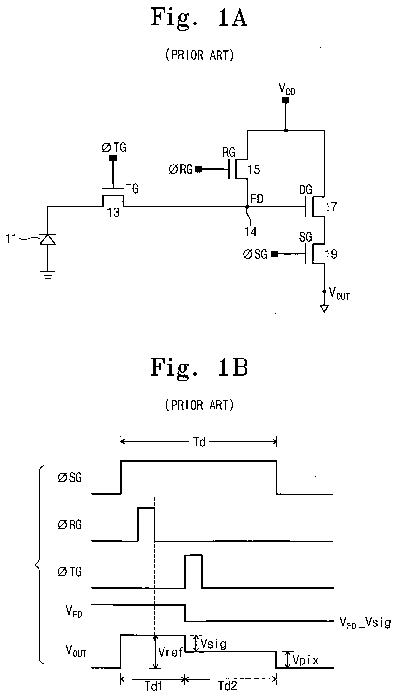
[0062] First, referring to FIG. 6A, each of the pixels of the image sensor according to the invention is comprised of a photo-receiving device 61, a transfer transistor 63 having stacked gate structure, a reset transistor 65, a drive transistor 67, and a selection transistor 69. The transfer transistor 63 includes a stacked gate structure formed of the transfer gate TG, the high-dielectric film, and the boosting gate BG. The boosting gate BG may be electrically connected to the selection gate SG of the selection transistor 69. The transfer transistor 63 transfers the signal charges that are generated at the photo-receiving device 61, to the floating diffusion region 64.

[0063] Referring to FIG. 6B, a first selection voltage φSG1 is applied to the selection gate SG of the selection transistor 69 during the first signal output phase Td1 (t0˜t3) of the signal output period, which turns the selection transistor 69 ON. After turning the selection transistor 69 ON (at t0), the reset voltag...

second embodiment

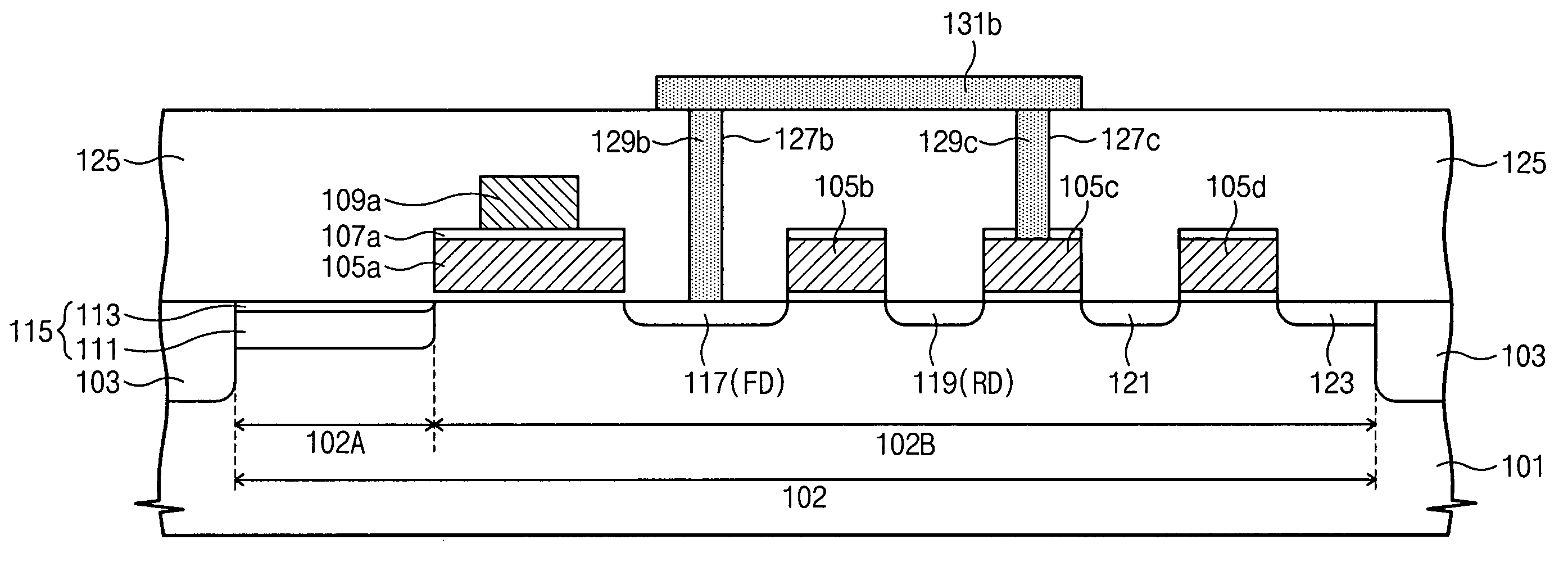
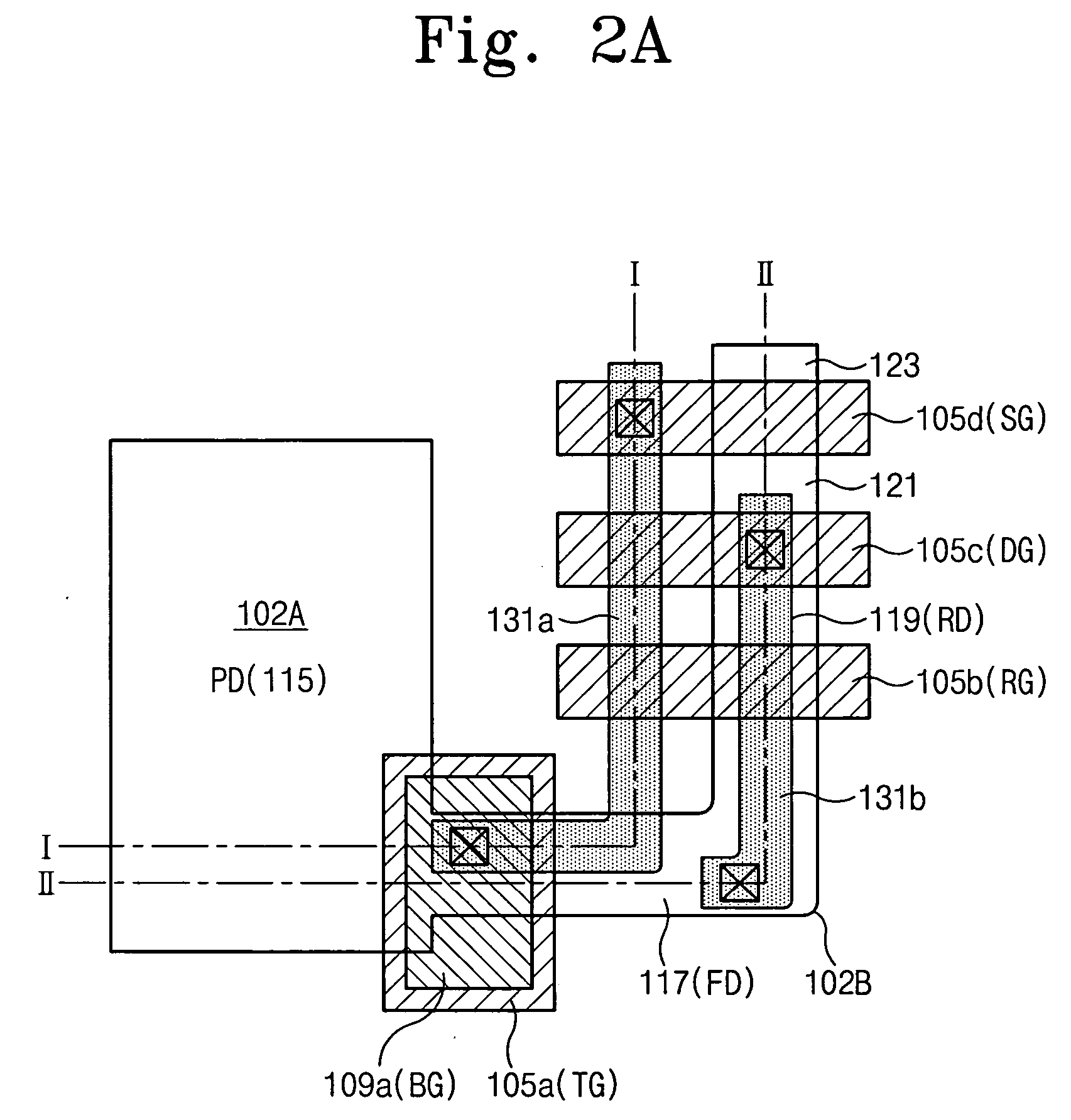
[0071] In the first exemplary embodiment aforementioned (FIG. 2A), the boosting gate may additionally be disposed over the drive gate 105c with interposing the dielectric film (and electrically connected to the selection gate 105d). And, likewise, in the second embodiment aforementioned (FIG. 5A), the boosting gate may be also disposed over the transfer gate 105c with an interposing dielectric film (and electrically connected to the selection gate 105d).

[0072] Moreover, in the first and second embodiments described above, the boosting gate may be also provided over the reset gate with an interposing dielectric film and connected to the selection gate. In this case, the boosting gate over the reset gate acts as a dummy gate without any bias voltage applied thereto.

[0073] A method of fabricating the image sensor including pixels having the structure shown in FIGS. 2A through 2C will now be described with reference to FIGS. 8A through 13A and 8B through 13B.

[0074]FIGS. 8A through 13A...


PUM


Abstract

Disclosed is a image sensor (e.g., a CMOS image sensor) including pixels each having a transfer transistor and a drive transistor, in which the gate of at least one of the transistors has a boosting gate disposed over it comprised of a conductive film pattern with interposing an insulation film. Thus, a voltage applied to the boosting gate is capacitively coupled to at least one of the transfer gate of the transfer transistor and a drive gate of the drive transistor. The transfer gate is supplied with the sum of the transfer voltage and the boosting gate-coupling voltage as a result and there is no need for providing a high voltage generator for the image sensor. The dynamic range of operation may be enhanced if such a coupling voltage is applied to the drive gate of the drive transistor.

Description

CROSS-REFERENCE TO RELATED APPLICATIONS [0001] This U.S. non-provisional patent application claims priority under 35 U.S.C. § 119 of Korean Patent Application 2005-05007 filed on Jan. 19, 2005, the entire contents of which are hereby incorporated by reference. BACKGROUND [0002] 1. Field of the Invention [0003] The present invention relates to image sensors, and more particularly relates to CMOS image sensors and methods of operating and fabricating the same. [0004] 2. Description of the Related Art [0005] The rapid advancement of digital camera technology and a resulting increase of their popularity has made high performance digital cameras in high demand among consumer electronics. The basic components of a digital camera that determine its performance level are an optical lens and an image sensor. The image sensor functions to transform light applied thereto (through the optical lens) into an electronic signal representing an image. [0006] A typical image sensor is composed of a p...

Claims


Application Information

Patent Timeline
Patent Type & Authority Applications(United States)
IPC IPC(8): H01L31/062H01L27/146H04N5/335H04N5/357H04N5/369H04N5/374H04N101/00
CPCH01L27/14609H01L27/14632H01L27/14656H01L27/14687H04N5/3597H04N5/3745H04N25/626H04N25/77E01H1/053
Inventor PARK, YOUNG-HOONPARK, WON-JEOH, TAE-SEOKSONG, JAE-HO
Owner SAMSUNG ELECTRONICS CO LTD
Why Eureka
Try Eureka