
Circuit for distributing a test signal applied to a pad of an electronic device

Active Publication Date: 2006-08-31
STMICROELECTRONICS SRL
View PDF20 Cites 0 Cited by
  • Summary
  • Abstract
  • Description
  • Claims
  • Application Information

AI Technical Summary

Benefits of technology

[0008] Studies carried out for overcoming this drawback confirmed that by internally connecting together replicated pads having the same function would cause unacceptable propagation delays during the normal operation of the device, but that could be tolerable during a test phase. Indeed, these propagation delays are relatively short compared to the time generally required for testing electronic devices.
[0009] Therefore, differently from what is commonly accepted by skilled persons, it is convenient to internally short-circuit replicated pads, provided that short-circuiting electrical paths be eventually opened after testing such that normal functioning of the finished device will not suffer intolerable propagation delays of the signals.

Problems solved by technology

Studies carried out for overcoming this drawback confirmed that by internally connecting together replicated pads having the same function would cause unacceptable propagation delays during the normal operation of the device, but that could be tolerable during a test phase.
Indeed, these propagation delays are relatively short compared to the time generally required for testing electronic devices.
During the normal functioning of the device, the circuit remains disabled.

Method used


Image

  • Circuit for distributing a test signal applied to a pad of an electronic device
  • Circuit for distributing a test signal applied to a pad of an electronic device
  • Circuit for distributing a test signal applied to a pad of an electronic device

Examples


Embodiment Construction

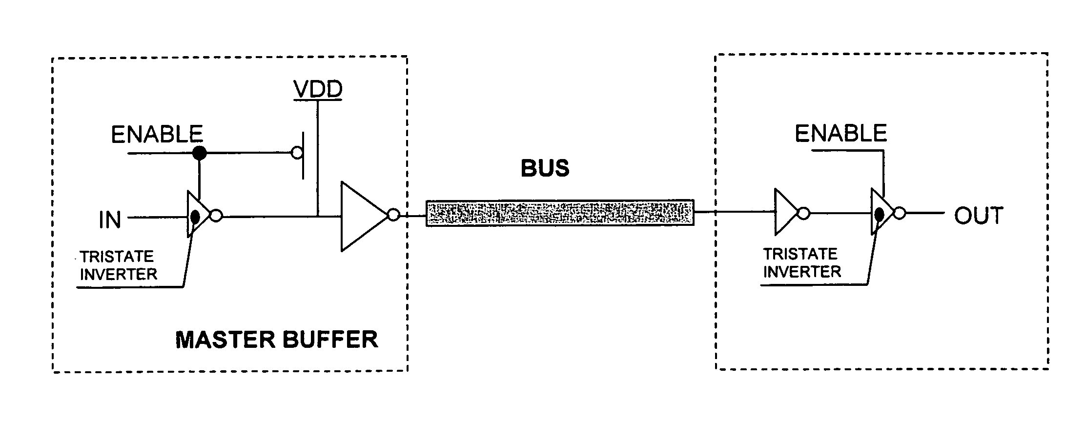
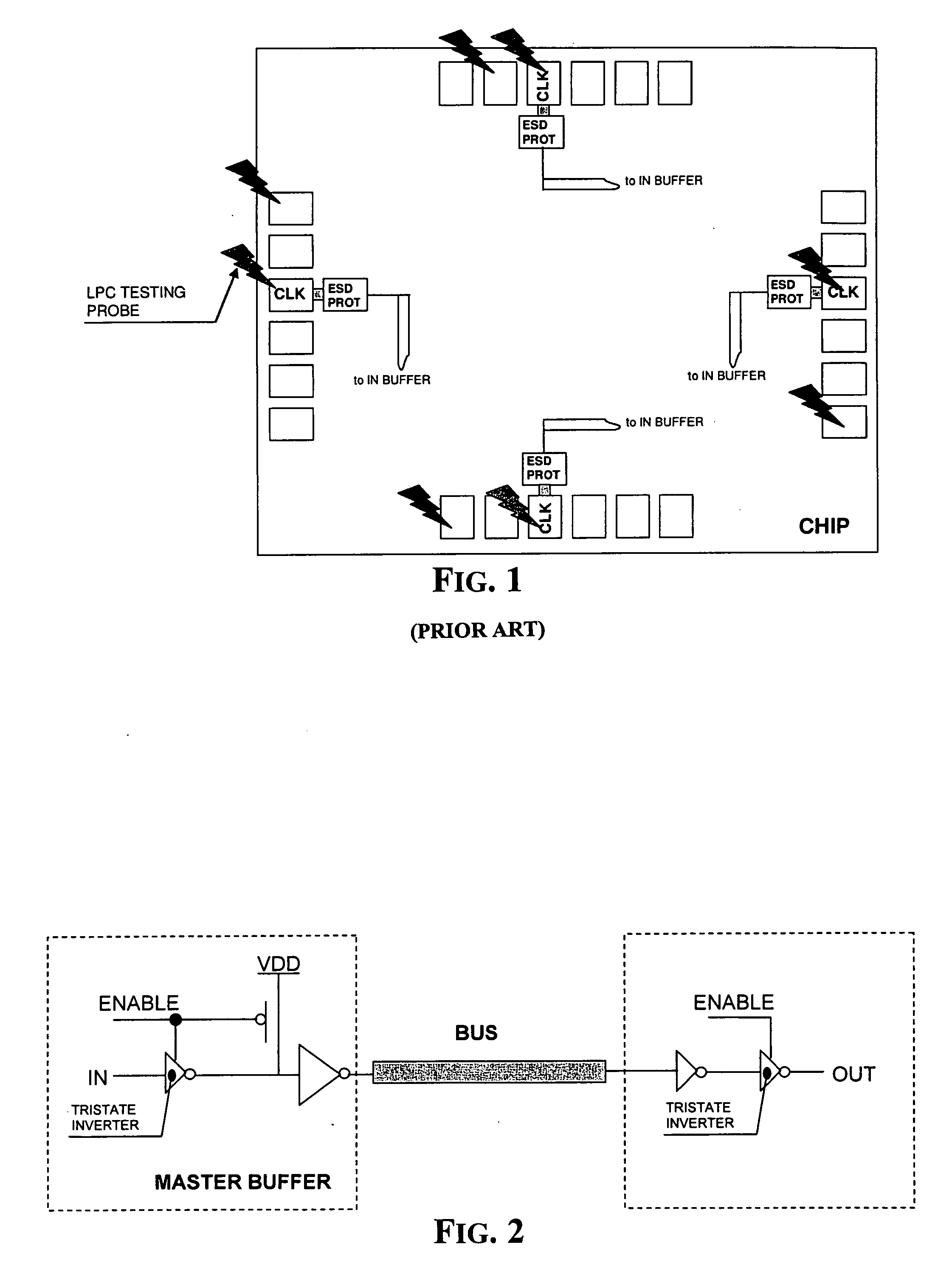
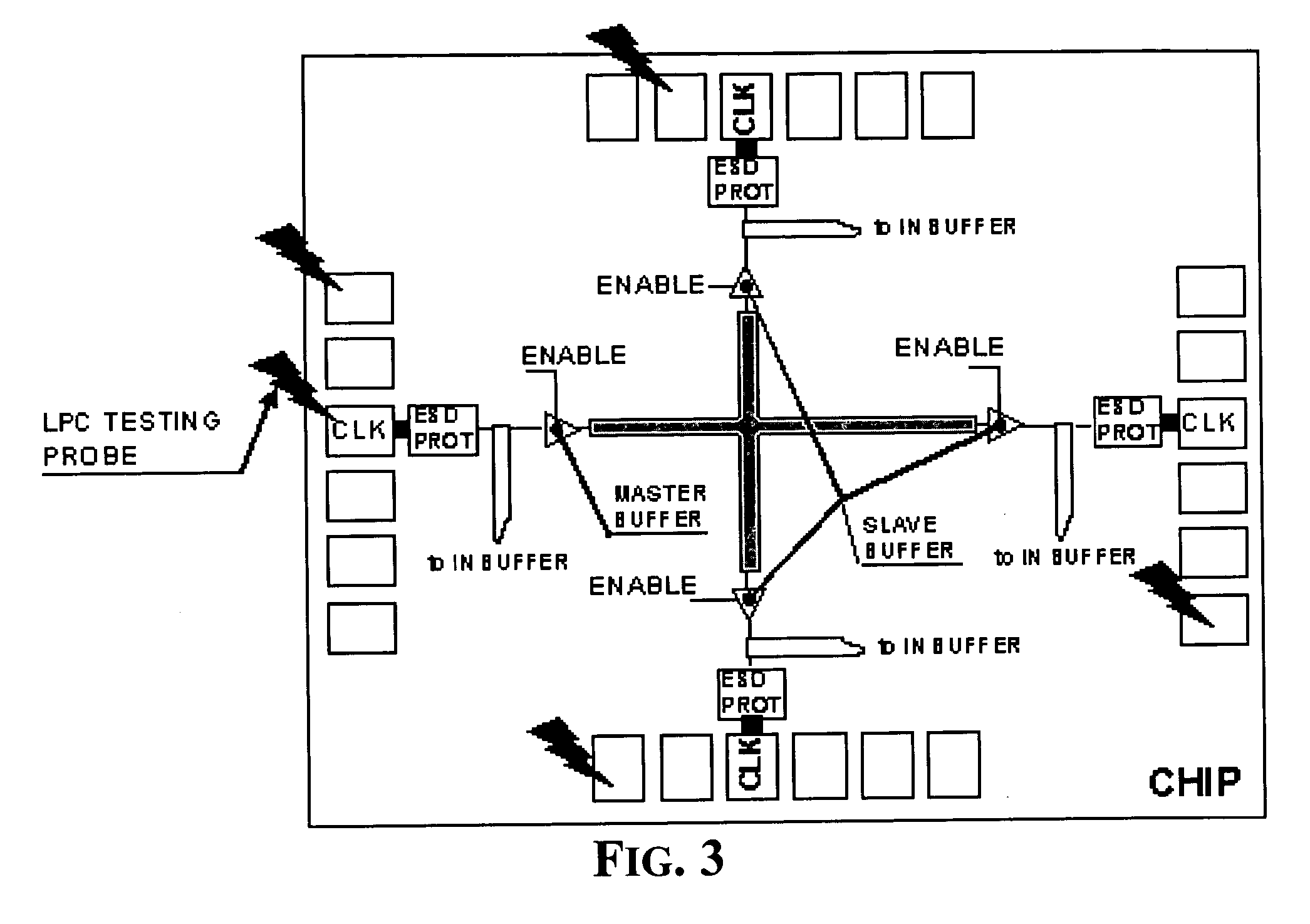
[0017] A test signal distribution circuit of this invention is shown in FIG. 2. It includes a “master” buffer and of one or more “slave” buffers connected to the “master” buffer via an interconnection bus. A test signal is fed on an input IN of the “master” buffer by applying it to a pad contacted by the tip of a probe during a test on wafer phase, and the master buffer transfers it on the interconnection bus when the master buffer is enabled by the enabling signal ENABLE.

[0018] The distribution circuit has as many “slave” buffers as the replicated pads of the “first” pad. Each of these “slave” buffers, enabled by the same signal ENABLE, makes the signal present on the interconnection bus available at the output OUT. The signal distribution circuit of this invention is connected to the pads of the device to be tested such that the input of the “master” buffer is connected to the “first” pad, while the output of each “slave” buffer replicates the signal present on the interconnectio...


PUM


Abstract

The circuit distributes a test signal applied to a pad of an electronic device that is enabled during test phases of the device and disabled during normal functioning. The circuit includes a “master” buffer, one or more “slave” buffers, one for each replicated pad, and an interconnection bus of the “master” and “slave” buffers. During a test phase, the “master” buffer replicates on the interconnection bus the test signal fed to a pad of the device, while the “slave” buffers convey to the various replica pads of the feed pad the signal present on the interconnection bus. During the normal operation of the device, the circuit remains disabled.

Description

FIELD OF THE INVENTION [0001] The present invention relates to the field of integrated circuits, and more particularly to techniques for testing electronic devices. BACKGROUND OF THE INVENTION [0002] Demand for electronic devices capable of implementing ever more numerous functions has led toward chips with an ever increasing number of connection pins. As a consequence, the time required for testing monolithically fabricated devices on a silicon wafer has increased proportionally with the number of pins of each device. Typically, there may be about 500 memory chips realized on a single 8-inch wafer and it is evident that verifying one memory chip at the time would require too much time. [0003] For this reason, techniques have been devised for parallel testing the individual chips on the wafer. In practice, test devices having a plurality of conducting probes are used. The tips of the probes are in contact with different pads of a plurality of devices realized on wafer, and through t...

Claims


Application Information

Patent Timeline
IPC IPC(8): G01R31/28
CPCG01R31/31723
Inventor GATTO, NICOLA DELGERACI, ANTONIOSFORZIN, MARCOROSITO, NICOLA
Owner STMICROELECTRONICS SRL
Learn More