Multi-bank random access memory structure with global and local signal buffering for improved performance

a random access memory and global and local signal technology, applied in the field of multi-bank random access memory (ram) structures, can solve the problems of increasing the resistance-capacitance (rc) time constant of the lines (i.e., wires) which form such global connectors, affecting the performance of the network, and causing poor slew rate, etc., to achieve fast slew, improve performance, and short propagation delay

Active Publication Date: 2013-11-28
GLOBALFOUNDRIES US INC
View PDF0 Cites 4 Cited by
  • Summary
  • Abstract
  • Description
  • Claims
  • Application Information

AI Technical Summary

Benefits of technology

[0005]In view of the foregoing, disclosed herein are embodiments of a multi-bank random access memory (RAM) structure (e.g., a multi-bank embedded dynamic random access memory (eDRAM) structure or a multi-bank static random access memory (SRAM) structure) that provides signal buffering at both the global and local connector level for improved performance. Specifically, inverters are incorporated into the global connector(s), which traverse groups of memory banks, and also into alternating groups of local connectors, which connect nodes on the global connector(s) to corresponding groups of memory banks, such that any signals (e.g., address signals, control signals or data signals) that are received by the memory banks from the memory controller via the global and local connectors are buffered by an even number of inverters and are thereby true signals. Signal buffering at both the global and local connector level in this manner results in relatively fast slews, short propagation delays, and low peak power consumption with minimal, if any, increase in area consumption.

Problems solved by technology

Unfortunately, as scaling continues through and beyond the 32 nm technology node, the resistance-capacitance (RC) time constant of the lines (i.e., wires) which form such global connectors has increased.
This increase in the RC time constant negatively impacts the ability of the global connectors, which are relatively long, to adequately drive the signals from the memory controller to the memory banks (i.e., to drive the signal to the multiple circuit loads) and, thereby results in poor slew rates.
The added buffers improve the slew rates, but do so at the expense of increased area consumption, increased peak power consumption and increased latency.
Signal buffering at both the global and local connector level in this manner results in relatively fast slews, short propagation delays, and low peak power consumption with minimal, if any, increase in area consumption.

Method used


Image

  • Multi-bank random access memory structure with global and local signal buffering for improved performance
  • Multi-bank random access memory structure with global and local signal buffering for improved performance
  • Multi-bank random access memory structure with global and local signal buffering for improved performance

Examples


Embodiment Construction

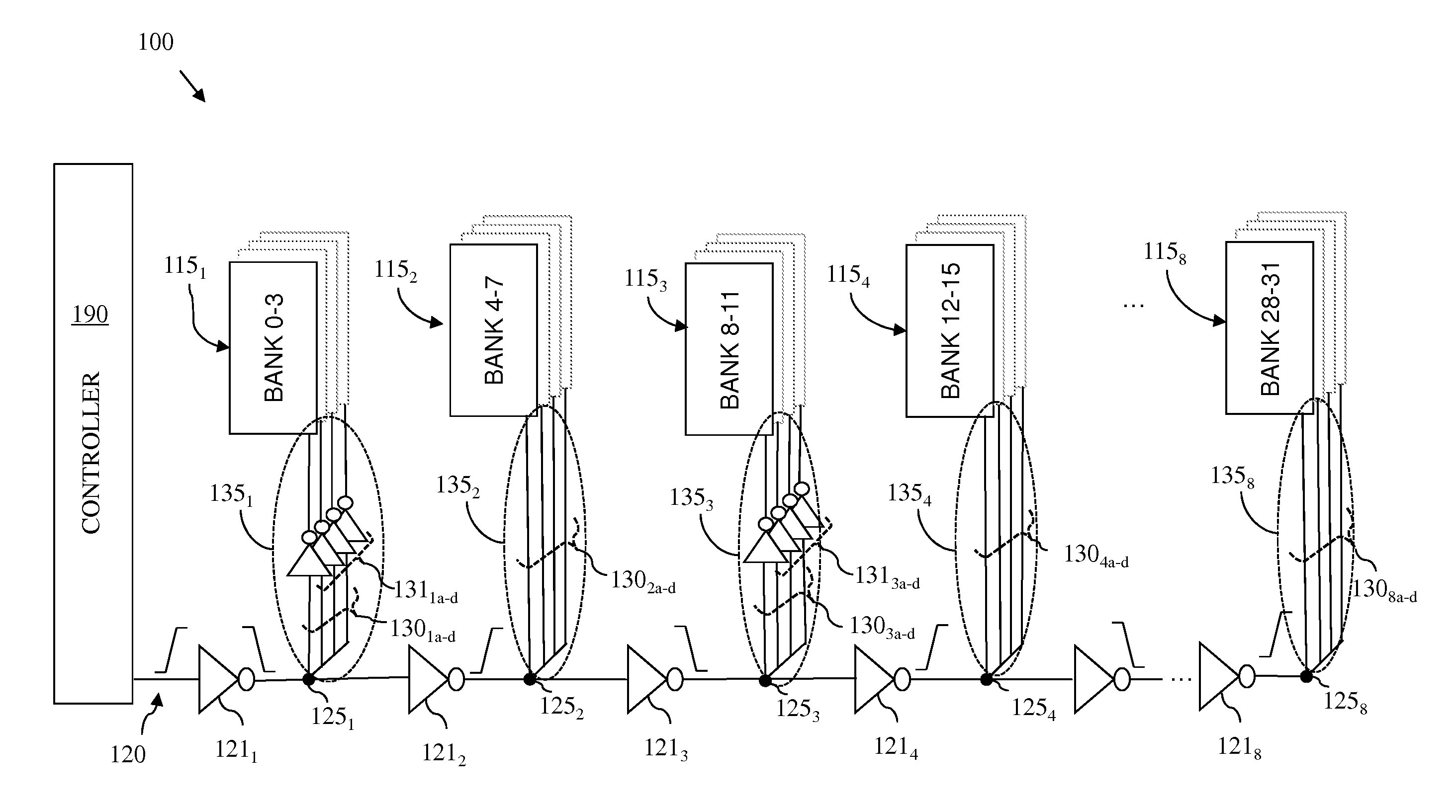
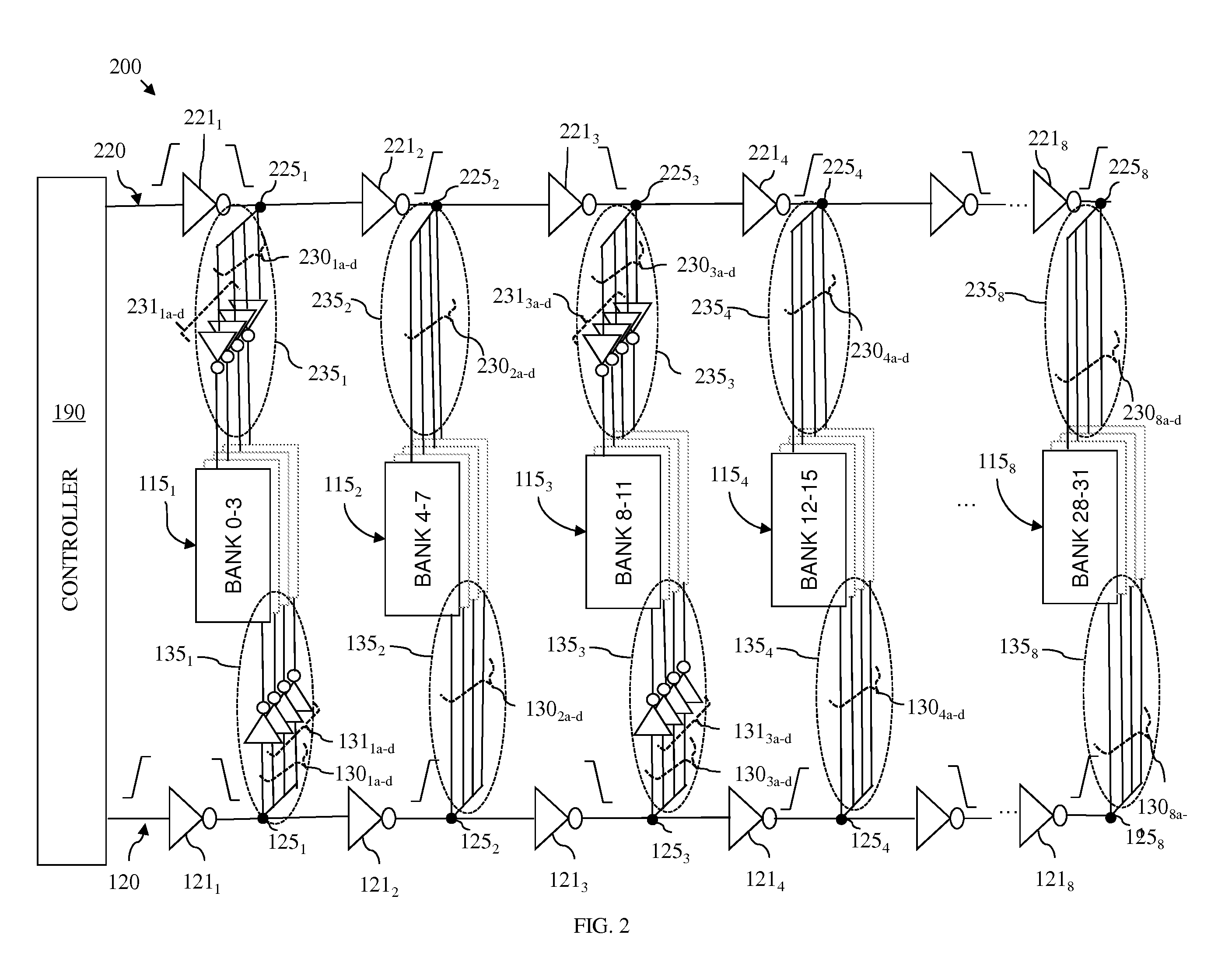
[0015]As mentioned above, in multi-bank random access memory (RAM) structures, such as multi-bank embedded dynamic random access memory (eDRAM) structures and multi-bank static random access memory (SRAM) structures, the performance of the global connectors, which carry signals (e.g., control signals, address signals and data signals) from a memory controller to the local connectors for the various memory banks, is critical to overall memory performance (i.e., memory timing parameters, such as slew and propagation delay). Unfortunately, as scaling continues through and beyond the 32 nm technology node, the resistance-capacitance (RC) time constant of the lines (i.e., wires) which form such global connectors has increased. This increase in the RC time constant negatively impacts the ability of the global connectors, which are relatively long, to adequately drive the signals from the memory controller to the memory banks (i.e., to drive the signal to the multiple circuit loads) and, t...


PUM


Abstract

Disclosed are embodiments of a multi-bank random access memory (RAM) structure that provides signal buffering at both the global and local connector level for improved performance. Specifically, inverters are incorporated into the global connector(s), which traverse groups of memory banks and which transmit signals (e.g., address signals, control signals, and/or data signals) from a memory controller, and also into alternating groups of local connectors, which connect nodes on the global connector(s) to corresponding groups of memory banks, such that any of the signals that are received by the memory banks from the memory controller via the global and local connectors are buffered by an even number of inverters and are thereby true signals. Signal buffering at both the global and local connector level results in relatively fast slews, short propagation delays, and low peak power consumption with minimal, if any, increase in area consumption.

Description

BACKGROUND[0001]1. Field of the Invention[0002]The present disclosure relates to multi-bank random access memory (RAM) structures and, more specifically, to embodiments of a multi-bank random access memory (RAM) structure (e.g., a multi-bank embedded dynamic random access memory (eDRAM) structure or a multi-bank static random access memory (SRAM) structure) with a combination of global and local signal buffering (e.g., global and local control, address, and data signal buffering) for improved performance.[0003]2. Description of the Related Art[0004]In multi-bank random access memory (RAM) structures, such as multi-bank embedded dynamic random access memory (eDRAM) structures and multi-bank static random access memory (SRAM) structures, the performance of the global connectors, which carry signals (e.g., control signals, address signals and data signals) from a memory controller to the local connectors for the various memory banks, is critical to overall memory performance (i.e., to ...

Claims


Application Information

Patent Timeline
Patent Type & Authority Applications(United States)
IPC IPC(8): G11C8/00
CPCG11C5/025G11C8/12G11C7/10G11C7/1048G11C7/18G11C11/4097
Inventor ANAND, DARREN L.FIFIELD, JOHN A.JACUNSKI, MARK D.LANAHAN, MATTHEW C.
Owner GLOBALFOUNDRIES US INC
Why Eureka
Try Eureka