Nonvolatile semiconductor memory device and method of fabricating the same

a semiconductor memory and non-volatile technology, applied in the field of semiconductor memory devices, can solve the problems of floating-gate memory devices losing charge, devices losing data, microscopic step differences

Active Publication Date: 2006-09-14
SAMSUNG ELECTRONICS CO LTD
View PDF13 Cites 73 Cited by
  • Summary
  • Abstract
  • Description
  • Claims
  • Application Information

AI Technical Summary

Problems solved by technology

Volatile memory devices lose their data when their power supply is interrupted or suspended, while the nonvolatile memory devices retain their data without power.
A floating-gate memory device may lose charge due to defects in the tunneling insulation film isolating the floating gate from the semiconductor substrate.
This process inevitably causes microscopic step differences, such that the top surfaces of the field isolation films 9 are positioned minutely higher than the top surface of the active regions of the semiconductor substrate 1.
This problem may become more serious as the memory cell sizes become smaller and the edges of the active region occupy a high percentage of the area of the cell structure.

Method used


Image

  • Nonvolatile semiconductor memory device and method of fabricating the same
  • Nonvolatile semiconductor memory device and method of fabricating the same
  • Nonvolatile semiconductor memory device and method of fabricating the same

Examples


Embodiment Construction

[0027] Example embodiments of the present invention will be described below in more detail with reference to the accompanying drawings. The present invention may, however, be embodied in different forms and should not be limited to the embodiments set forth herein. Rather, these embodiments are provided so that this disclosure will thoroughly and completely convey the scope of the invention to those skilled in the art.

[0028] The thickness of layers and regions in the figures are exaggerated for clarity. When a layer is referred to as being on another layer or substrate, it may be directly on the other layer or substrate, or may contain intervening layers. Like numerals refer to like elements throughout the specification.

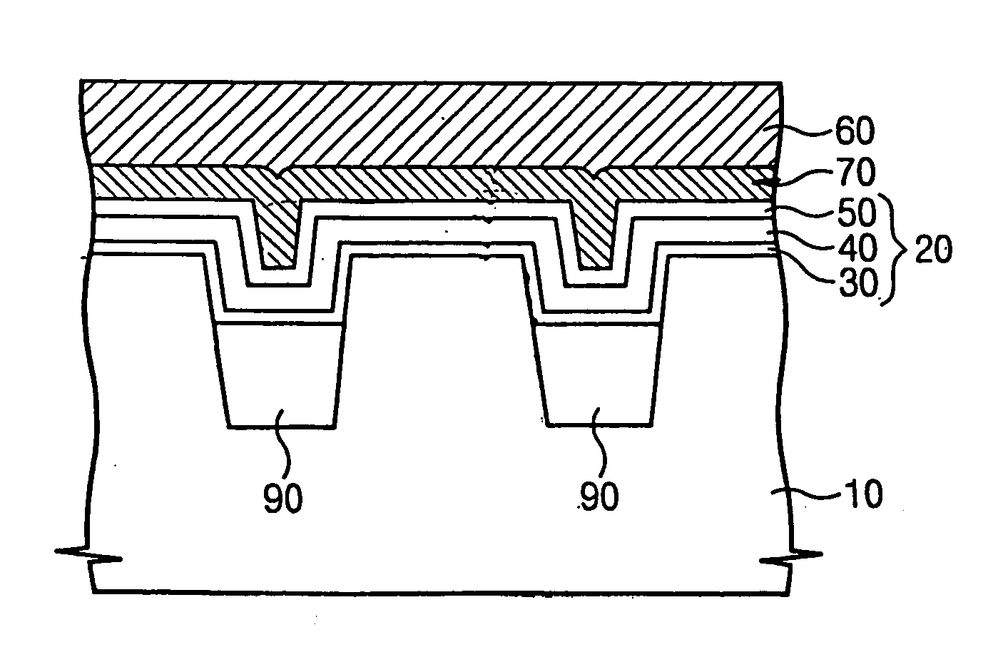
[0029]FIGS. 4A through 4D are sectional diagrams of nonvolatile semiconductor memories, taken along the direction of gate length, in accordance with various embodiments of the invention.

[0030] In FIG. 4A, field isolation films 90 are formed in the semiconductor su...


PUM


Abstract

In an example embodiment, a semiconductor substrate has a plurality of active regions separated by a plurality of trenches. A gate insulation film fills at least a portion of the trenches, and a conductive gate film is formed over the gate insulation film. In an example embodiment, the gate insulation film, may include a tunneling insulation film, a charge storage film, and a blocking insulation film. The example embodiment may also include field isolation films, which partially fill the trenches of the semiconductor substrate, such that the upper surfaces of the active regions or the substrate are higher than the upper surfaces of the field isolation films.

Description

CROSS-REFERENCE TO RELATED APPLICATIONS [0001] This U.S. non-provisional patent application claims priority under 35 U.S.C. § 119 of Korean Patent Application 2005-21070 filed on Mar. 14, 2005, the entire contents of which are hereby incorporated by reference. BACKGROUND [0002] The present invention relates to semiconductor devices, and more particularly to a nonvolatile semiconductor memory device and method of fabricating the same. [0003] Semiconductor memory devices are widely employed to store various data in electronic systems, normally classified into volatiles and nonvolatiles. Volatile memory devices lose their data when their power supply is interrupted or suspended, while the nonvolatile memory devices retain their data without power. Therefore, nonvolatile memory devices are widely used in applications such as mobile telephones, memory cards, storing audio or image files, and other portable devices in operational environments without a wired power supply. [0004] Nonvolati...

Claims


Application Information

Patent Timeline
Patent Type & Authority Applications(United States)
IPC IPC(8): H01L29/94
CPCH01L27/115H01L27/11568H01L29/42332H01L29/7881H01L29/792H10B69/00H10B43/30
Inventor LEE, CHANG-HYUN
Owner SAMSUNG ELECTRONICS CO LTD
Why Eureka
Try Eureka