Plasma display device and method of treating the same

Inactive Publication Date: 2007-01-04
FUJITSU HITACHI PLASMA DISPLAY LTD
View PDF9 Cites 2 Cited by
  • Summary
  • Abstract
  • Description
  • Claims
  • Application Information

AI Technical Summary

Benefits of technology

[0010] It is an object of the present invention to provide a plasma display device capable of exactly correcting luminance degradation in a color-wise manner, and a method of treatment therefor.

Problems solved by technology

Plasma display devices suffer from degradation of individual phosphors for red, green and blue colors.
Difference in degrees of degradation from color to color has been causative of changes in the white balance, and has resulted in degradation of image quality.
The gain correction solely based on the cumulative values of operation time, however, cannot reflect difference in load-induced degradation of video luminance, and fails in exactly estimating the luminance degradation characteristics.
Problems also reside in that accumulation of the number of application of the effective pulses for discharge for the individual cells may increase the cost due to expansion of circuit configuration and addition of a memory device, and reside in difficulty of ensuring storage time in the memory device.
Still another problem resides in that changes in lifetime characteristics ascribable to difference in the effective pulse voltage for discharge are not reflected, so that the luminance degradation characteristics cannot be estimated in a more exact manner.

Method used


Image

  • Plasma display device and method of treating the same
  • Plasma display device and method of treating the same
  • Plasma display device and method of treating the same

Examples


Embodiment Construction

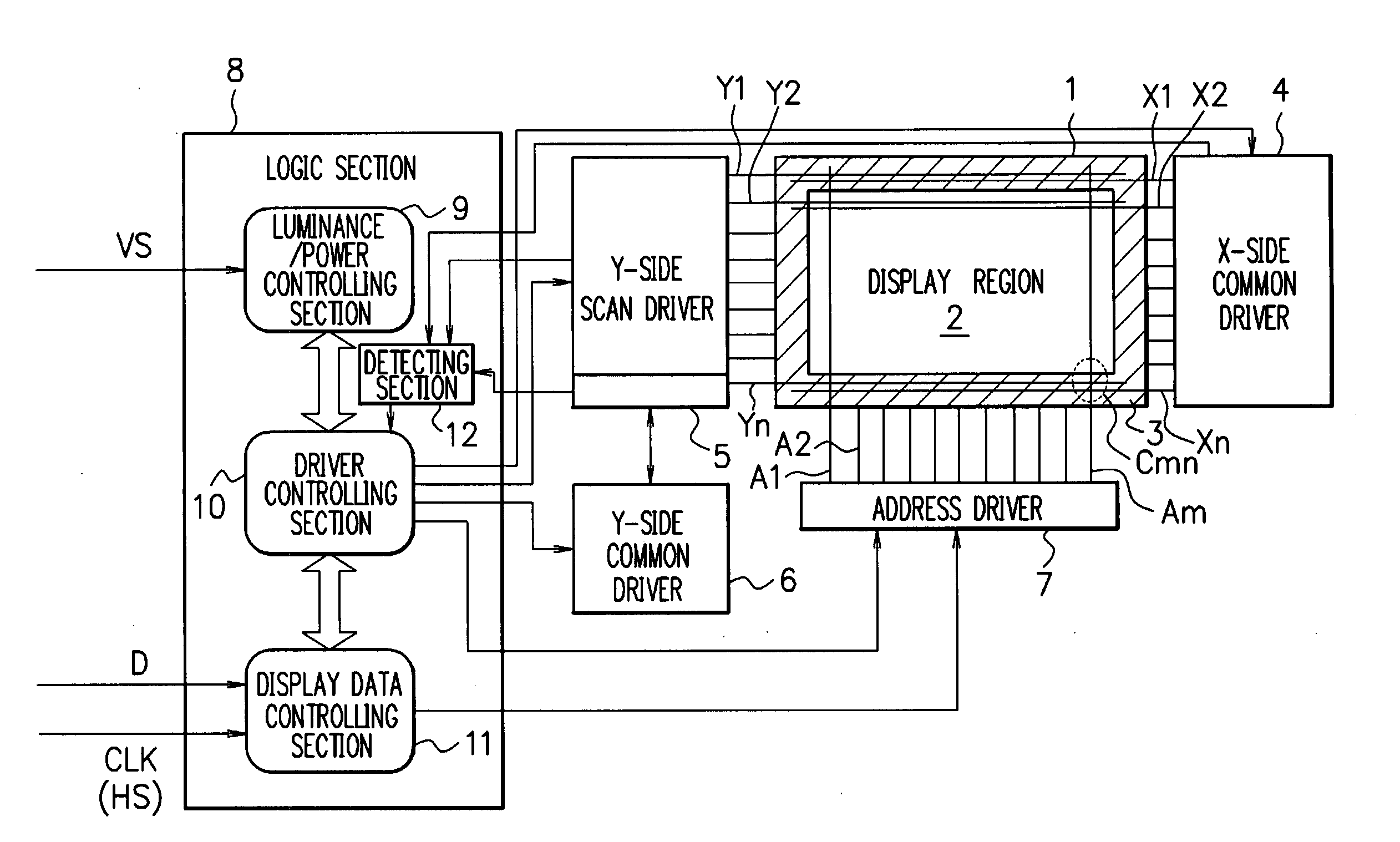
[0035]FIG. 1 is a drawing showing and exemplary configuration of the plasma display device according to an embodiment of the present invention. The plasma display device of this embodiment has scanning electrodes (display electrodes) Y1 to Yn and display electrodes X1 to Xn parallel to each other, and address electrode A1 to Aj provided normal to (so as to cross) these electrodes Y1 to Yn, and X1 to Xn. The display electrodes X1 to Xn are provided as being corresponded to, and in the vicinity of the scanning electrode Y1 to Yn, respectively.

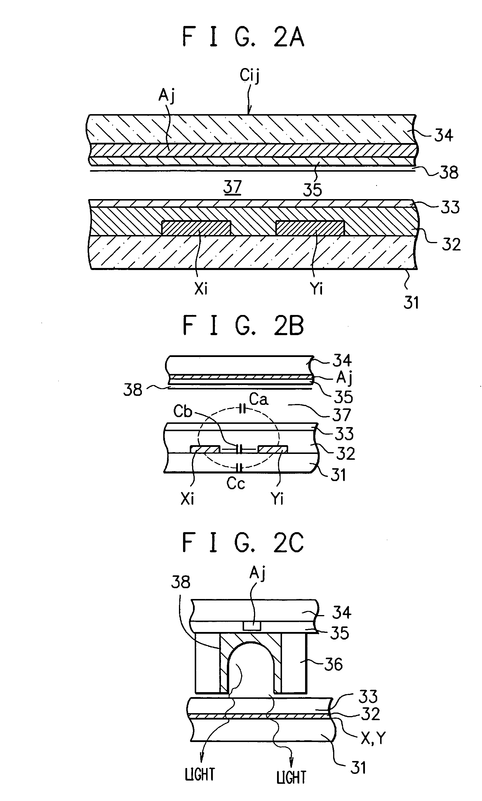
[0036] The display panel 1 has a plurality of cells arranged in a form of a matrix of m rows and n columns. Each cell Cij is composed of an intersection of a scanning electrode Y1 and an address electrode Aj, and an adjacent display electrodes Xi corresponded thereto. The cell Cij corresponds to one pixel of a displayed image, and thereby the display panel 1 can present a two-dimensional image.

[0037] The display panel 1 has a display region 2 a...


PUM


Abstract

Aiming at more exactly correcting luminance degradation in a color-wise manner, a plasma display device proposed herein has a gain correction section color-wisely correcting gains of video signals for a plurality of colors; and a plasma display panel presenting display corresponding to the gain-corrected video signals while being supplied with sustain pulses, wherein the gain correction section color-wisely corrects gains of the video signals, corresponding to time corresponded to the operation time, video load ratio, and the number of the sustain pulses or values relevant thereto.

Description

CROSS-REFERENCE TO RELATED APPLICATIONS [0001] This application is based upon and claims the benefit of priority from the prior Japanese Patent Application Nos. 2005-178219, filed on Jun. 17, 2005 and 2006-122403, filed on Apr. 26, 2006, the entire contents of which are incorporated herein by reference. BACKGROUND OF THE INVENTION [0002] 1. Field of the Invention [0003] The present invention relates to a plasma display device and a method of treating the same. [0004] 2. Description of the Related Art [0005] Plasma display devices suffer from degradation of individual phosphors for red, green and blue colors. Difference in degrees of degradation from color to color has been causative of changes in the white balance, and has resulted in degradation of image quality. Patent Document 1 listed below discloses a plasma display device configured as correcting gains of the individual amplifiers for RGB corresponding to cumulative values of operation time. Patent Document 2 listed below disc...

Claims


Application Information

Patent Timeline
IPC IPC(8): G09G3/28G09G3/20G09G3/288G09G3/291G09G3/294G09G3/298H04N5/66
CPCG09G3/2022G09G3/288G09G3/294G09G2330/02G09G2320/0285G09G2320/043G09G2320/0666G09G2320/0242G09G3/296
Inventor MIYAZAKI, YOSHINORINOGUCHI, YASUJITAJIMA, MASAYAKOJIMA, AYAHITO
Owner FUJITSU HITACHI PLASMA DISPLAY LTD
Why Eureka
Try Eureka