

Integrated circuit device and electronic instrument
a technology of integrated circuits and electronic instruments, applied in the direction of instruments, semiconductor devices, electrical devices, etc., can solve the problem of becoming difficult to mount the integrated circuit devices
Active Publication Date: 2007-01-04
SEIKO EPSON CORP
View PDF99 Cites 64 Cited by
- Summary
- Abstract
- Description
- Claims
- Application Information
AI Technical Summary
Problems solved by technology
Therefore, if the chip size is reduced by merely shrinking the integrated circuit device as the display d
Method used
View moreImage
Smart ImageViewing Examples

Examples
 PUM
 Abstract
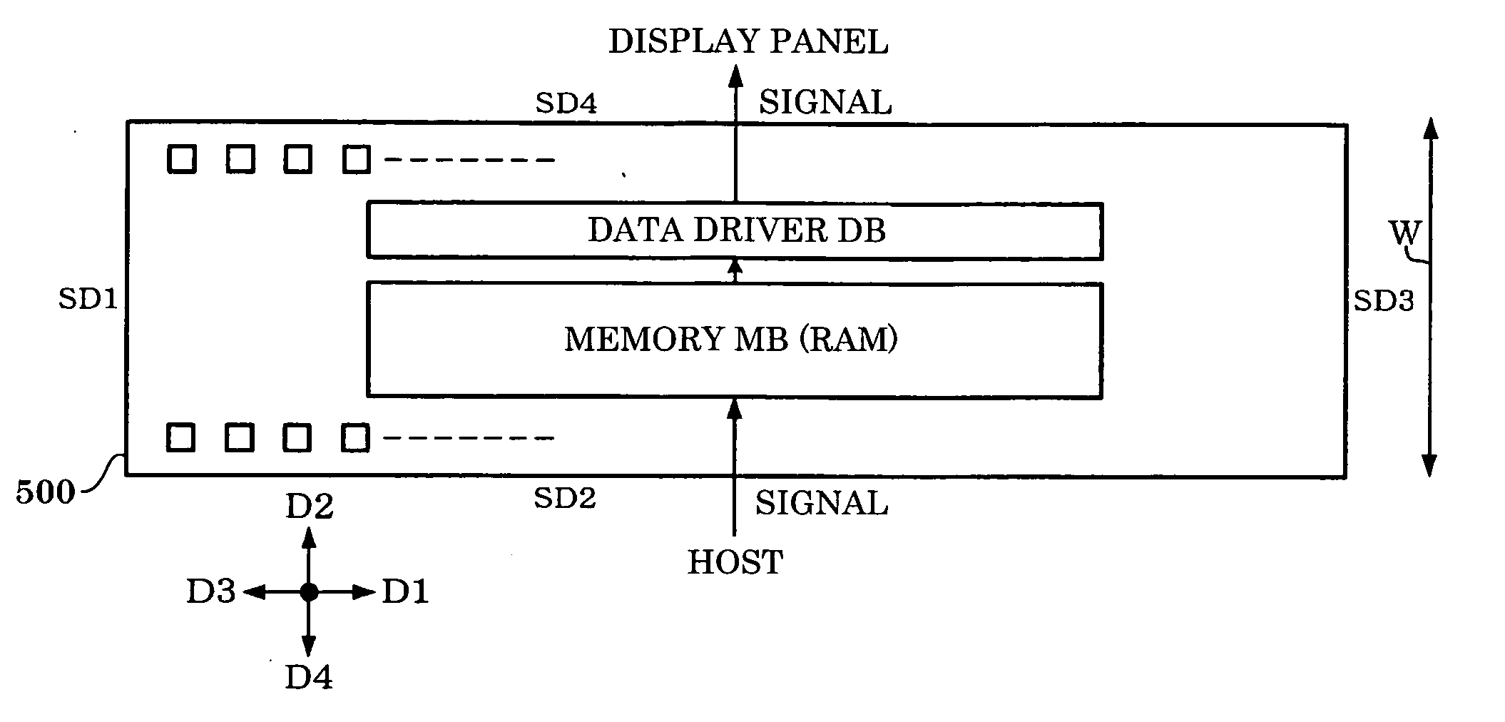
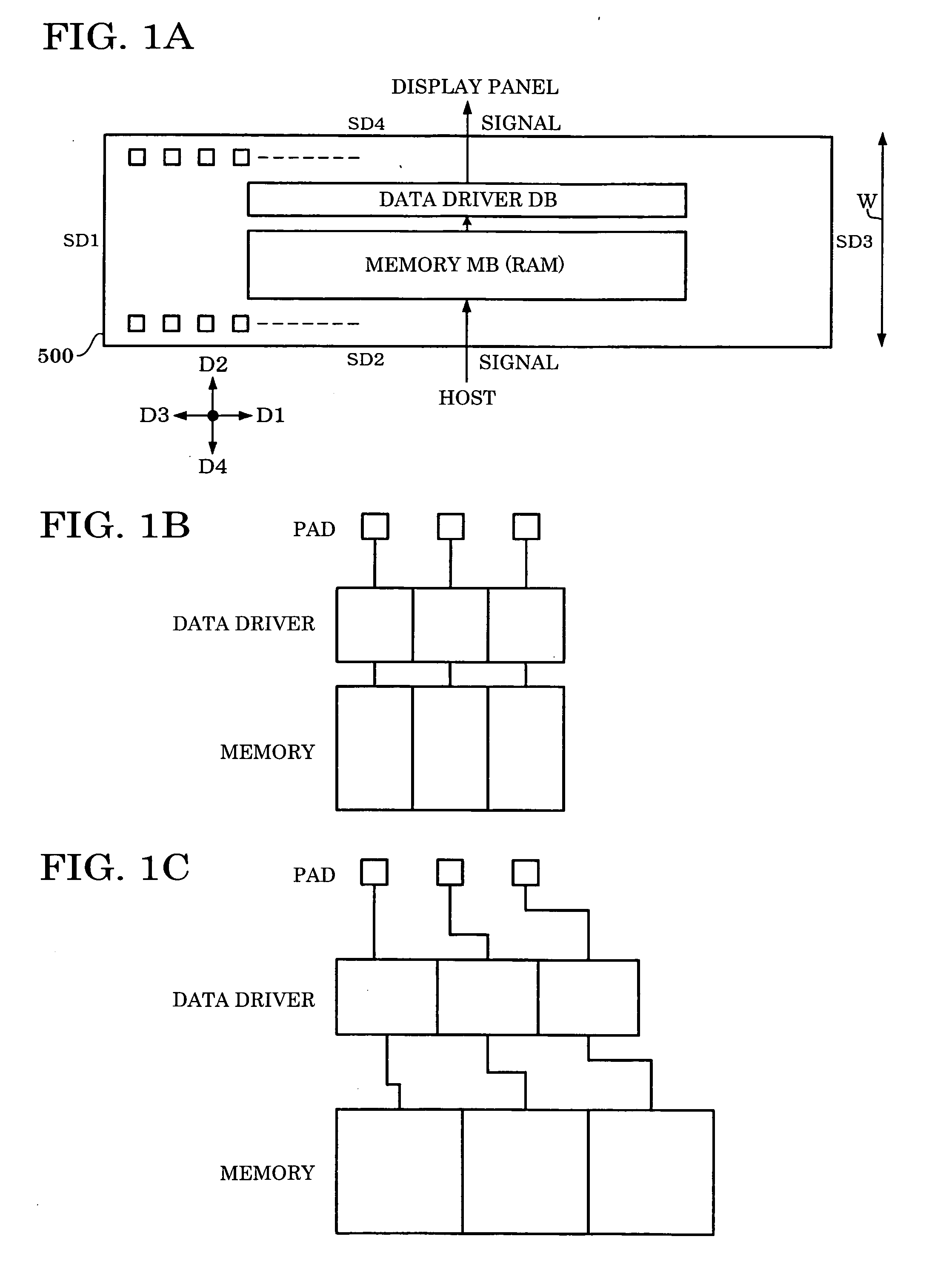
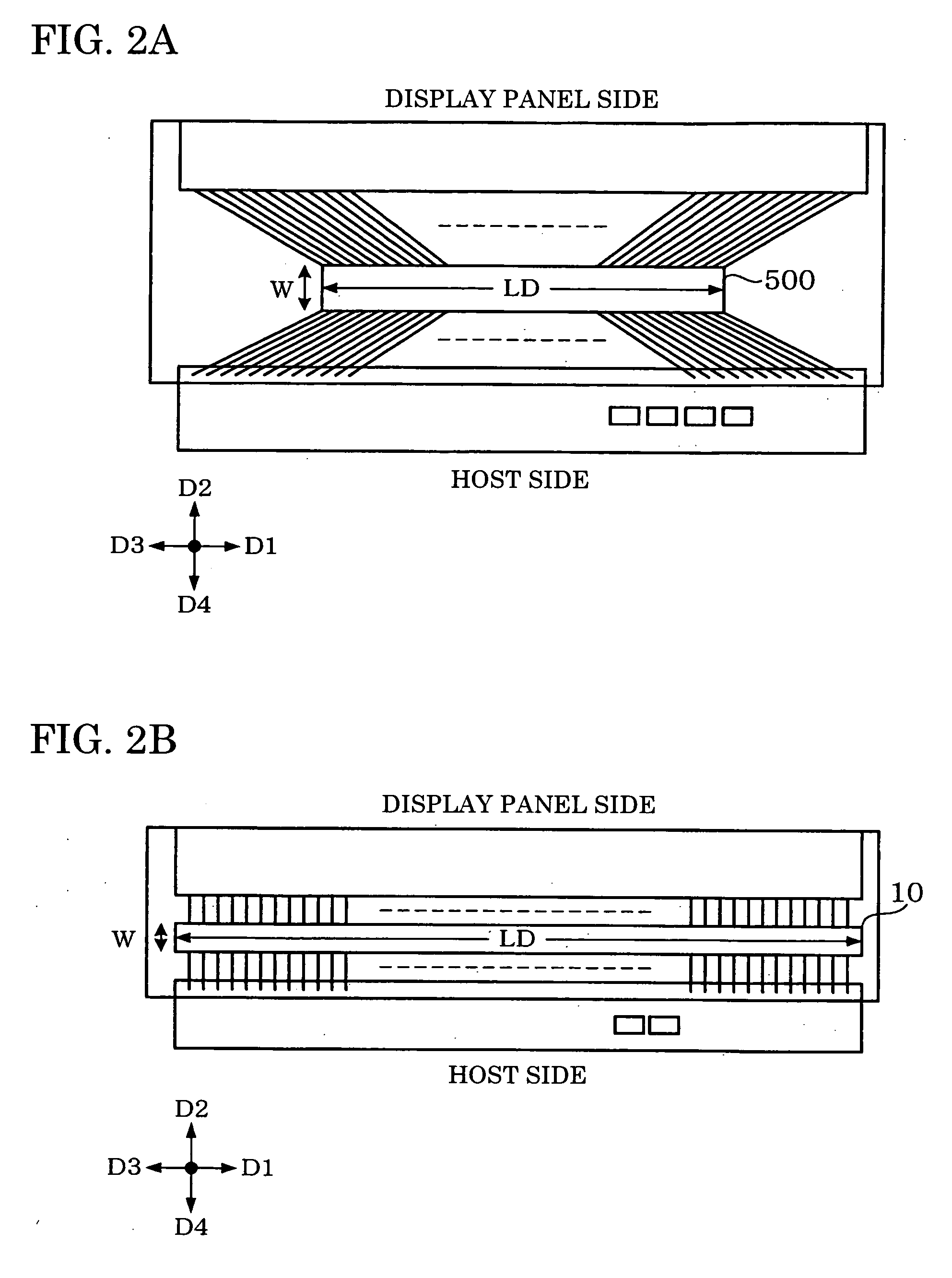
An integrated circuit device includes first to Nth circuit blocks CB1 to CBN, a first interface region disposed along a fourth side and on the D2 side of the first to Nth circuit blocks CB1 to CBN, and a second interface region disposed along a second side and on the D4 side of the first to Nth circuit blocks CB1 to CBN. A local line LLG formed using a wiring layer lower than an Ith layer is provided between the adjacent circuit blocks as at least one of a signal line and a power supply line. Global lines GLG and GLD formed using the Ith or higher wiring layer are provided along the direction D1 over the circuit block disposed between the nonadjacent circuit blocks as at least one of a signal line and a power supply line.
Description
[0001] Japanese Patent Application No. 2005-192479, filed on Jun. 30, 2005, and Japanese Patent Application No. 2006-34500, filed on Feb. 10, 2006, are hereby incorporated by reference in their entirety. BACKGROUND OF THE INVENTION [0002] The present invention relates to an integrated circuit device and an electronic instrument. [0003] A display driver (LCD driver) is an example of an integrated circuit device which drives a display panel such as a liquid crystal panel (JP-A-2001-222249). A reduction in the chip size is required for the display driver in order to reduce cost. [0004] However, the size of the display panel incorporated in a portable telephone or the like is almost constant. Therefore, if the chip size is reduced by merely shrinking the integrated circuit device as the display driver by using a microfabrication technology, it becomes difficult to mount the integrated circuit device. SUMMARY [0005] A first aspect of the invention relates to an integrated circuit device ...
Claims
Login to View More Application Information
Patent Timeline
 IPC IPC(8): G09G3/36
CPCG09G3/2011G09G3/3688H01L2224/05553G09G2330/04G09G2330/02G02F1/133
InventorITO, SATORUMORIGUCHI, MASAHIKOMAEKAWA, KAZUHIROITOMI, NOBORUKODAIRA, SATORUKARASAWA, JUNICHIKUMAGAI, TAKASHIISHIYAMA, HISANOBUFUJISE, TAKASHI
OwnerSEIKO EPSON CORP