

Integrated circuit device and electronic instrument
a technology of integrated circuits and electronic instruments, which is applied in the direction of instruments, semiconductor devices, electrical devices, etc., can solve the problems of difficult mounting of integrated circuit devices and difficult to provide products with desired characteristics
Inactive Publication Date: 2007-01-04
SEIKO EPSON CORP
View PDF99 Cites 56 Cited by
- Summary
- Abstract
- Description
- Claims
- Application Information
AI Technical Summary
Problems solved by technology
Therefore, if the chip size is reduced by merely shrinking the integrated circuit device as the display driver by using a microfabrication technology, it becomes difficult to mount the integrated circuit de
Method used
View moreImage
Smart ImageViewing Examples

Examples
 PUM
 Abstract
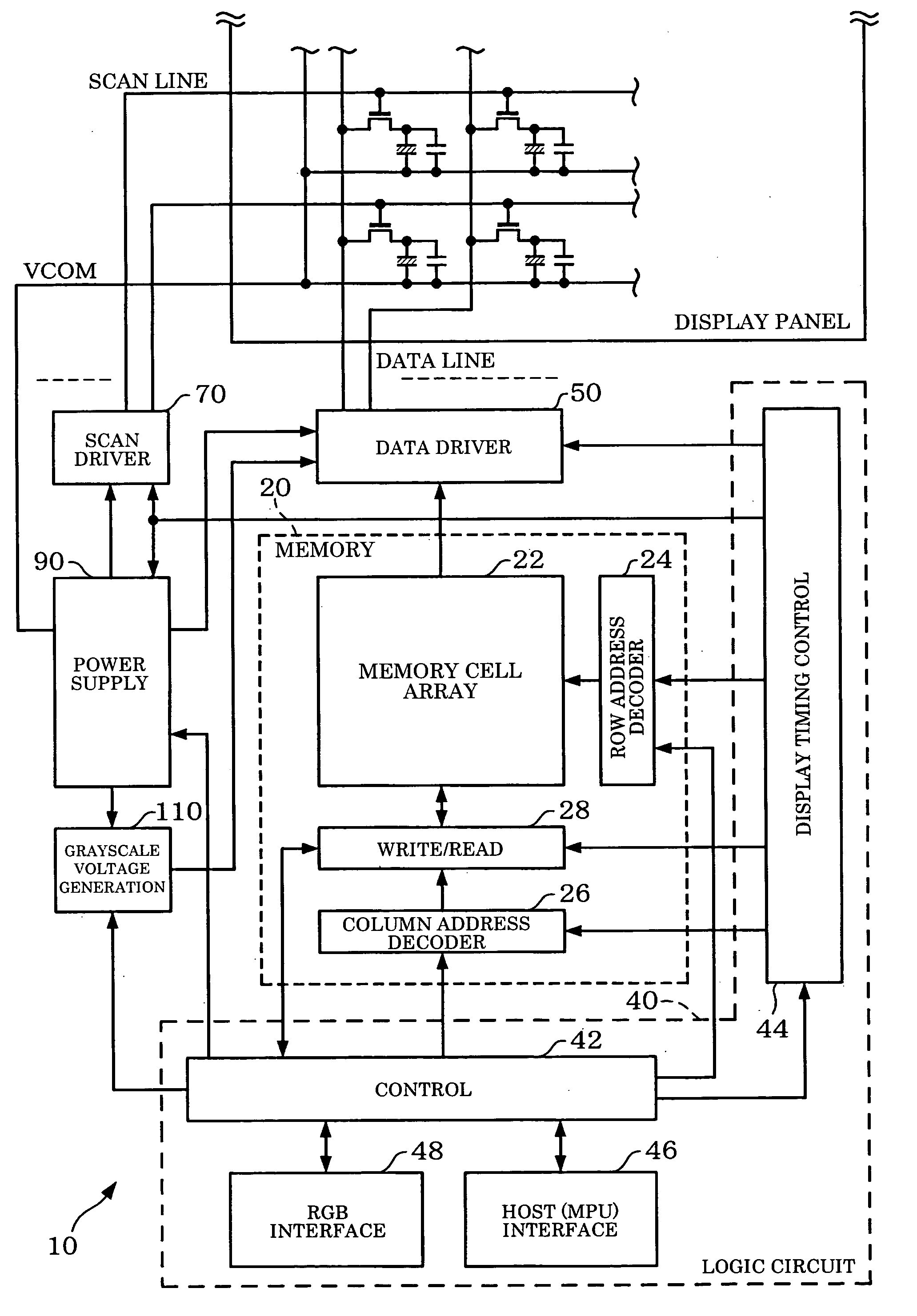
An integrated circuit device includes a scan driver block SB which generates a control signal for driving a scan line, a pad PDt electrically connected with the scan line, and transistors pDTrt and nDTrt of which a connection node DNDt is electrically connected with the PDt pad and which are push-pull connected between a high-potential-side power supply and a low-potential-side power supply. The transistors pDTrt and nDTrt are gate-controlled based on the control signal from the scan driver block SB. The pad PDt is disposed in an upper layer of at least one of the transistors pDTrt and nDTrt so that the pad PDt overlaps part or the entirety of at least one of the transistors pDTrt and nDTrt.
Description
[0001] Japanese Patent Application No. 2005-192479 filed on Jun. 30, 2005, Japanese Patent Application No. 2005-253388 filed on Sep. 1, 2005, and Japanese Patent Application No. 2005-253389 filed on Sep. 1, 2005, are hereby incorporated by reference in their entirety. BACKGROUND OF THE INVENTION [0002] The present invention relates to an integrated circuit device and an electronic instrument. [0003] A display driver (LCD driver) is an example of an integrated circuit device which drives a display panel such as a liquid crystal panel (JP-A-2001-222249). A reduction in the chip size is required for the display driver in order to reduce cost. [0004] However, the size of the display panel incorporated in a portable telephone or the like is almost constant. Therefore, if the chip size is reduced by merely shrinking the integrated circuit device as the display driver by using a microfabrication technology, it becomes difficult to mount the integrated circuit device. [0005] It is advantage...
Claims
Login to View More Application Information
Patent Timeline
 IPC IPC(8): G09G3/36
CPCG09G3/3674H01L27/0251G09G3/3696G09G3/3685
InventorKUMAGAI, TAKASHIISHIYAMA, HISANOBUMAEKAWA, KAZUHIROITO, SATORUFUJISE, TAKASHIKARASAWA, JUNICHIKODAIRA, SATORU
OwnerSEIKO EPSON CORP