Mos transistors having inverted t-shaped gate electrodes and fabrication methods thereof

a technology of mos transistor and gate electrode, which is applied in the direction of semiconductor devices, basic electric elements, electrical appliances, etc., can solve the problems of difficult to fully diffuse arsenic ions to the lower part, difficult to homogenously dope the first deformed gate pattern with arsenic ions, and the short channel characteristic of mos transistors may deteriora

Inactive Publication Date: 2007-05-03
SAMSUNG ELECTRONICS CO LTD
View PDF8 Cites 9 Cited by
  • Summary
  • Abstract
  • Description
  • Claims
  • Application Information

AI Technical Summary

Problems solved by technology

However, it may be difficult to homogenously dope the first deformed gate pattern with the arsenic ions because the lower diffusivity of the arsenic ions makes it difficult to fully diffuse the arsenic ions to the lower part of the first deformed gate pattern.
However, the long-time, high-temperature annealing process also acts to increase the depth of the n-type heavily-doped regions 51 such that the short channel characteristic of the NMOS transistor may deteriorate.
Also, when the second undoped gate pattern 41p is formed thinly, it may cause problems in the formation of the PMOS transistor.
This may cause instability in the threshold voltage characteristic of the PMOS transistor.

Method used


Image

  • Mos transistors having inverted t-shaped gate electrodes and fabrication methods thereof
  • Mos transistors having inverted t-shaped gate electrodes and fabrication methods thereof
  • Mos transistors having inverted t-shaped gate electrodes and fabrication methods thereof

Examples


Embodiment Construction

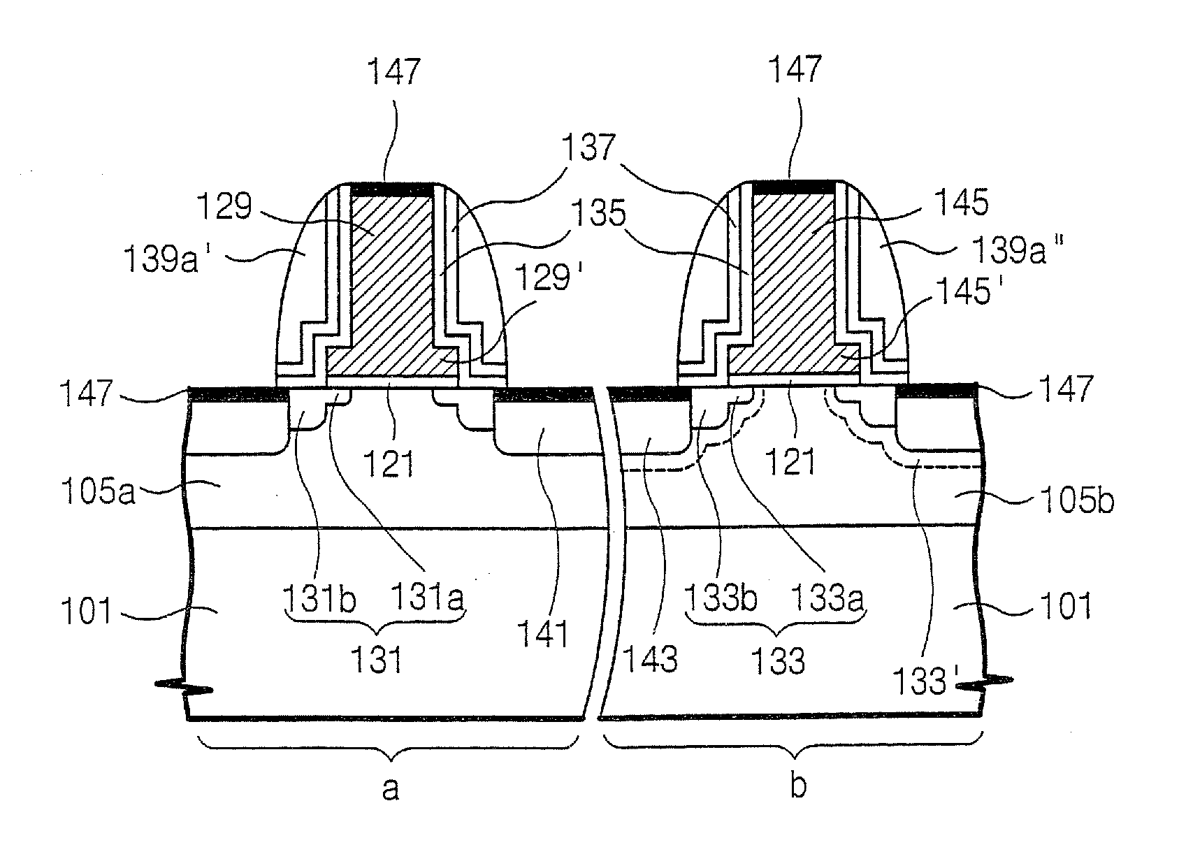
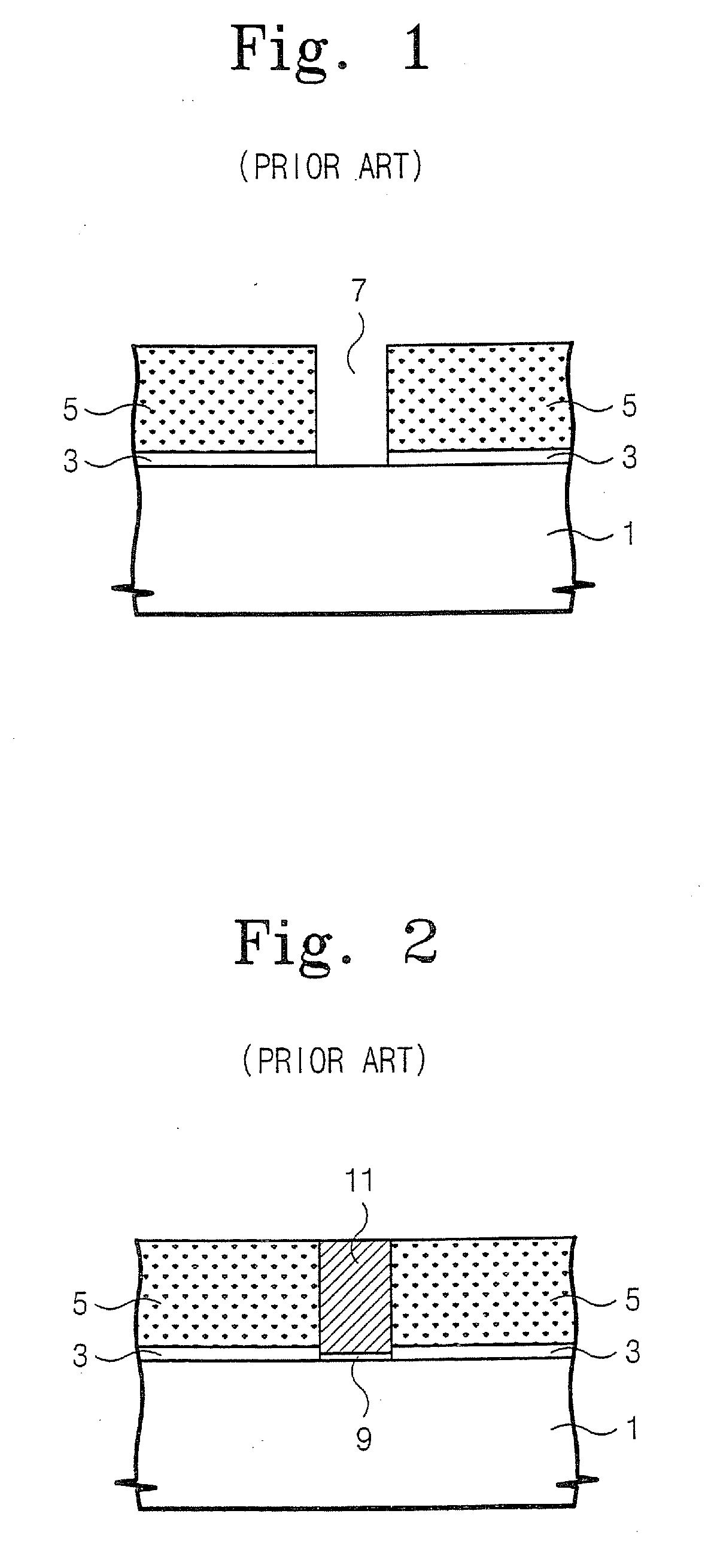
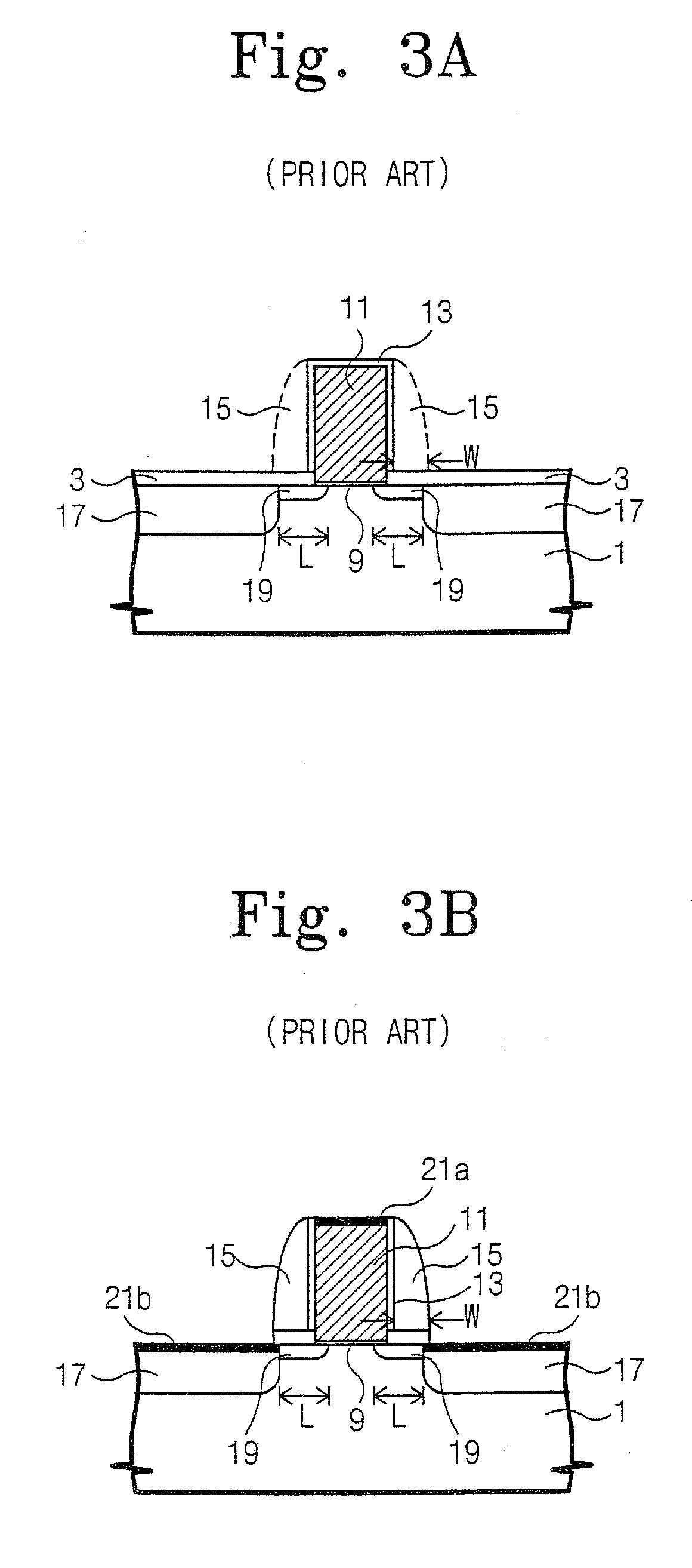
[0036] The present invention will now be described more fully with reference to the accompanying drawings, in which typical embodiments of the invention are shown. This invention, however, may be embodied in many different forms and should not be construed as limited to the embodiments set forth herein. Rather, these embodiments are provided so that this disclosure will be thorough and complete, and will fully convey the scope of the invention to those skilled in the art. In the drawings, the thickness of layers and regions are exaggerated for clarity. It will also be understood that when a layer or element is referred to as being “on” another layer or substrate, it can be directly on the other layer, element or substrate, or intervening layers and / or elements may also be present. In contrast, when a layer / element is referred to as being “directly on” another layer / element, there are no intervening layers or elements present. Likewise, when an element is described as being “between”...


PUM


Abstract

MOS transistors have an active region defined in a portion of a semiconductor substrate, a gate electrode on the active region, and drain and source regions in the substrate. First and second lateral protrusions extend from the lower portions of respective sidewalls of the gate electrode. The drain region has a first lightly-doped drain region under the first lateral protrusion, a second lightly-doped drain region adjacent the first lightly-doped drain region, and a heavily-doped drain region adjacent to the second lightly-doped drain region. The source region similarly has a first lightly-doped source region under the second lateral protrusion, a second lightly-doped source region adjacent the first lightly-doped source region, and a heavily-doped source region adjacent to the second lightly-doped source region. The second lightly-doped regions are deeper than the first lightly-doped regions, and the gate electrode may have an inverted T-shape.

Description

REFERENCE TO PRIORITY APPLICATION [0001] This application is a divisional of U.S. application Ser. No. 10 / 683,782, filed Oct. 10, 2003, which claims priority to Korean Application No. 2002-62009, filed Oct. 11, 2002. The disclosure of each of the above-referenced applications are hereby incorporated herein by reference.FIELD OF THE INVENTION [0002] The present invention relates to semiconductor devices, and, more specifically, to metal oxide semiconductor (MOS) transistors and fabrication methods thereof. BACKGROUND OF THE INVENTION [0003] MOS devices refer to integrated circuits that include numerous MOS transistors. One way of increasing the integration of MOS devices is to decrease the size of the MOS transistors. Various methods for decreasing the size of MOS transistors have been proposed, such as the method for fabricating a short channel MOS transistor disclosed in, U.S. Pat. No. 6,245,619 B1. FIGS. 1, 2, and 3A are cross-sectional views illustrating the method for fabricatin...

Claims


Application Information

Patent Timeline
Patent Type & Authority Applications(United States)
IPC IPC(8): H01L29/94H01L21/28H01L21/336H01L21/8238H01L29/423
CPCH01L21/28114H01L21/823842H01L21/82385H01L21/823864H01L29/42376H01L29/665H01L29/66537H01L29/66553H01L29/66583H01L21/18
Inventor LEE, SHIN-AEPARK, DONG-GUNLEE, CHANG-SUBCHOE, JEONG-DONGKIM, SUNG-MINKIM, SEONG-HO
Owner SAMSUNG ELECTRONICS CO LTD
Why Eureka
Try Eureka