Substrate processing method and substrate processing apparatus
- Summary
- Abstract
- Description
- Claims
- Application Information
AI Technical Summary
Benefits of technology
Problems solved by technology
Method used
Image


Examples
Embodiment Construction
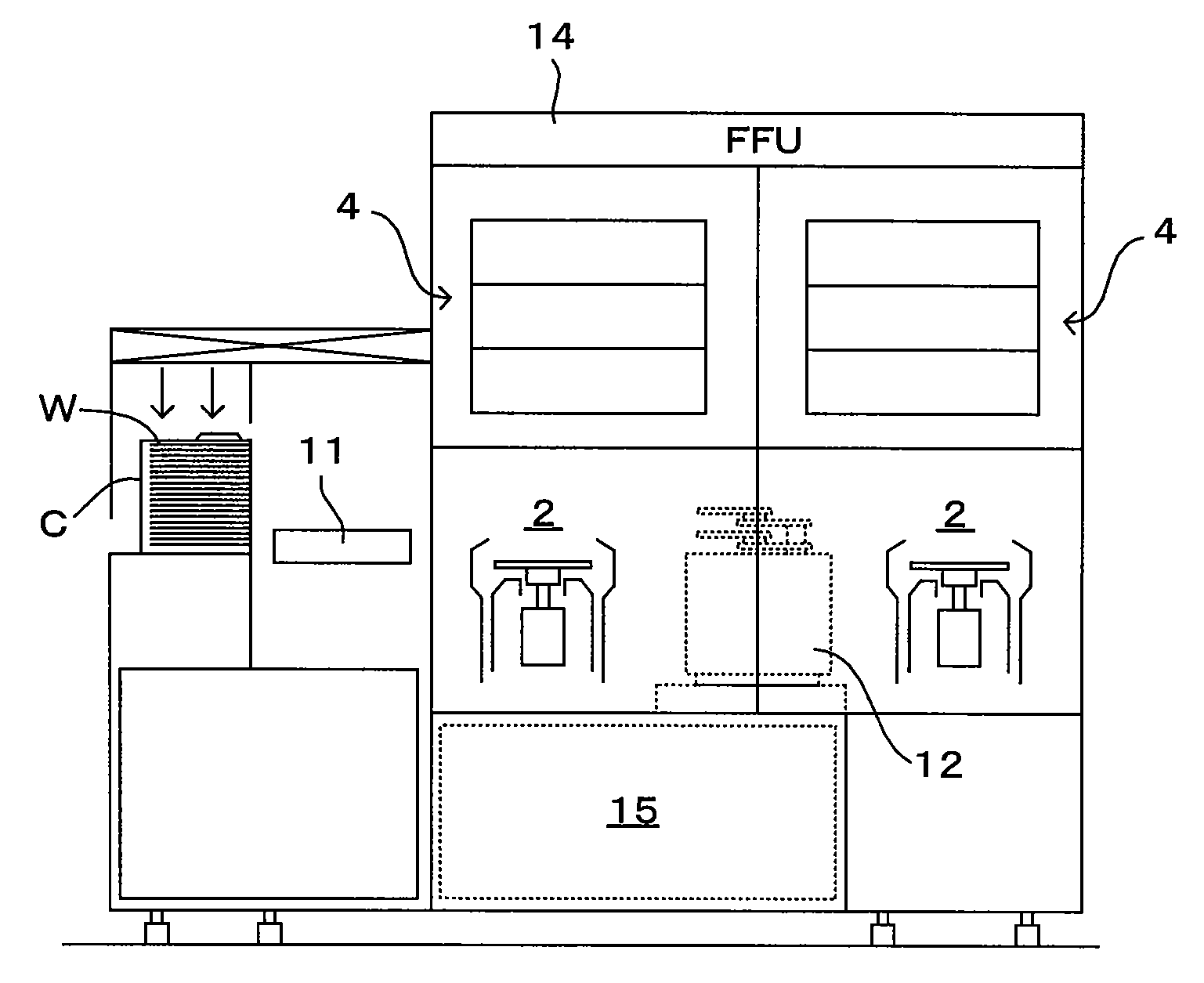
[0023]FIG. 1 is a layout plan view which illustrates an embodiment of a substrate processing apparatus according to the present invention and FIG. 2 is its side view. FIG. 3 is a block diagram which shows construction of a main controller. This substrate processing apparatus is a single-wafer type substrate processing apparatus that is used for the cleaning processes for the purpose of removing contaminants such as particles and various types of metallic impurities adhering to a surface (corresponds to “surface subjected to be processed” in the invention) of a substrate W, such as a semiconductor wafer, or the like. More specifically, this is an apparatus which removes contaminants together with frozen film, by applying a preprocessing liquid to the surface of the substrate on which device patterns are formed, thereby forming a film of the preprocessing liquid, then, freezing said liquid film and supplying post-processing liquid to the liquid film which is already frozen (frozen fil...
PUM
| Property | Measurement | Unit |
|---|---|---|
| Diameter | aaaaa | aaaaa |
| Freezing point | aaaaa | aaaaa |
| Surface temperature | aaaaa | aaaaa |
Abstract
Description
Claims
Application Information
 - R&D
- Intellectual Property
- Life Sciences
- Materials
- Tech Scout
- Unparalleled Data Quality
- Higher Quality Content
- 60% Fewer Hallucinations
Browse by: Latest US Patents, China's latest patents, Technical Efficacy Thesaurus, Application Domain, Technology Topic, Popular Technical Reports.
© 2025 PatSnap. All rights reserved.Legal|Privacy policy|Modern Slavery Act Transparency Statement|Sitemap|About US| Contact US: help@patsnap.com