Semiconductor integrated circuit and method for controlling the same

a technology of integrated circuits and semiconductors, applied in the field of semiconductor integrated circuits, can solve the problems of long time to save and restore in serial all the data held in the register, loss of internal state excluding nonvolatile memory,

Active Publication Date: 2007-06-28
RENESAS ELECTRONICS CORP
View PDF13 Cites 47 Cited by
  • Summary
  • Abstract
  • Description
  • Claims
  • Application Information

AI Technical Summary

Benefits of technology

[0023] Also, the operation method may be achieved by further issuing a first control signal after the internal state data is set to the plurality of sub scan chains; and supplying power to the target surface in response to the first control sig

Problems solved by technology

Usually, when the power supply to the semiconductor integrated circuit is stopped, an internal state is lost excluding a nonvolatile memory.
Therefore, it would tak

Method used


Image

  • Semiconductor integrated circuit and method for controlling the same
  • Semiconductor integrated circuit and method for controlling the same
  • Semiconductor integrated circuit and method for controlling the same

Examples


first embodiment

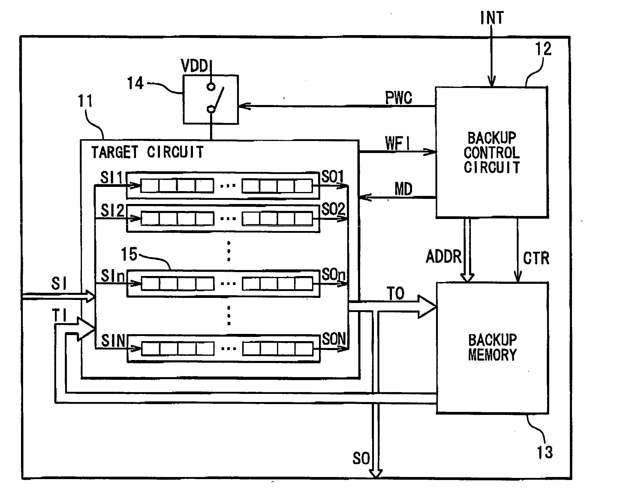
[0035]FIG. 1 is a block diagram showing the configuration of a semiconductor integrated-circuit according to the present invention. Referring to FIG. 1, the semiconductor integrated circuit includes a target circuit 11 whose internal state is saved as internal state data, a backup memory 13 which stores the internal state data of the target circuit 11, a backup control circuit 12 which controls a saving operation and restoring operation of the internal state data of the target circuit 11, and a switch 14 which controls power supply of the target circuit 11. The internal state of the target circuit 11 is restored based on internal state data held by flip-flops in the target circuit 11.

[0036] The backup control circuit 12 receives an instruction (WFI) from the target circuit 11, switches an operation mode (MD) of the target circuit 11, and saves data indicating the internal state of the target circuit 11, that is, the internal state data in the backup memory 13. Moreover, the backup c...

second embodiment

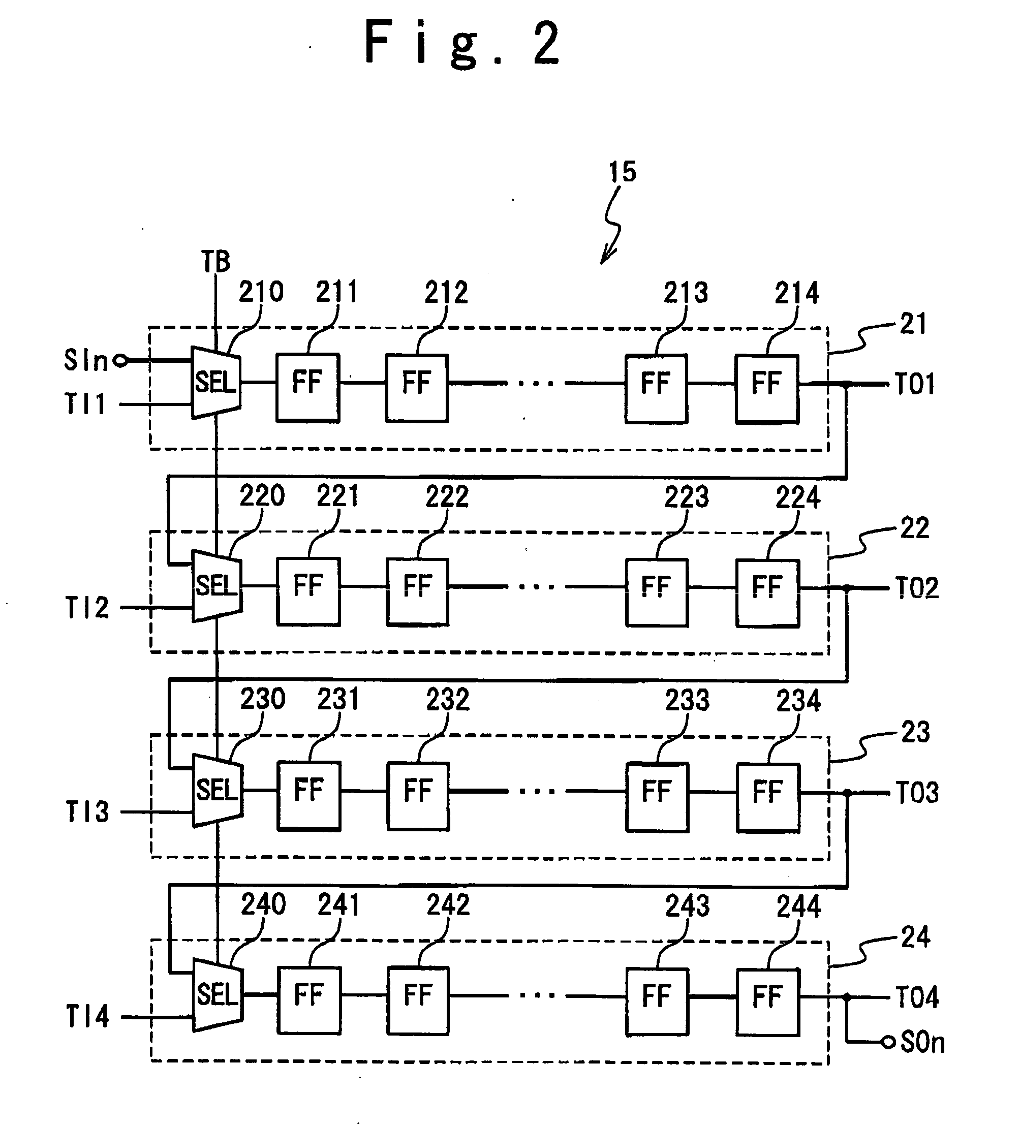
[0056]FIG. 4 is a block diagram showing the configuration of the scan chain in the semiconductor integrated circuit according to the present invention to shorten a minimum restoration time. The minimum restoration time is a time required to restore the initial state of the target circuit when the restoration of the internal state data is instructed immediate after the internal state data starts to be saved. In the scan chain 15 shown in FIG. 4, selector circuits are provided for the head portions of the sub scan chains 21 to 24 shown in FIG. 2. This scan chain 15 includes sub scan chains 31, 32, 33 and 34. The sub scan chain 31 includes selector circuits 319 and 310 and flip-flops 311 to 314. Similarly, the sub scan chain 32 includes selector circuits 329 and 320 and flip-flops 321 to 324, the sub scan chain 33 includes selector circuits 339 and 330 and flip-flops 331 to 334, and the sub scan chain 34 includes selector circuits 349 and 340 and flip-flops 341 to 344. The portion of t...

third embodiment

[0066]FIG. 6 is a block diagram showing an example of the scan chain 15 including the dummy flip-flops in the semiconductor integrated circuit according to the present invention. This dummy flip-flops belongs to other scan chains, and operate as a part of the other scan chains when the scan path is tested. The scan chain 15 shown in FIG. 6 does not include flip-flops 224 and 241 of the scan chain shown in FIG. 2. That is, the number of flip-flops included in sub scan chains 22 and 24 are less than that of the sub scan chains 21 and 23 in the scan chain 15 shown in FIG. 6. In the sub scan chain 22, a flip-flop 224 (called “dummy flip-flop” hereafter) not included in the scan chain 15 is connected after the flip-flop 223. Therefore, the flip-flop 223 is connected with the dummy flip-flop 224′ and the selector circuit 230 of the sub scan chain 23 in the next stage. The dummy flip-flop 224′ outputs the output data from the flip-flop 223 to the backup memory 13. Moreover, in the sub scan...


PUM


Abstract

A semiconductor integrated circuit includes a target circuit with at least a scan chain having sub scan chains of stages to sequentially shift a test data in response to a clock signal in a scan path test mode, and each of the sub scan chains includes first flip-flops connected in series. A backup control circuit controls the target circuit and a memory such that a plurality of sub internal state data of a data indicating an internal state of the target circuit are stored as a plurality of write data in the memory in a save mode through the sub scan chains and the plurality of sub internal state data are read out from the memory as a plurality of read data and set in the sub scan chains in a restore mode.

Description

BACKGROUND OF THE INVENTION [0001] 1. Field of the Invention [0002] The present invention pertains to a semiconductor integrated circuit and a method for controlling thereof. In particular, the present invention pertains to a semiconductor integrated circuit including a circuit that saves and restores the internal state of the semiconductor integrated circuit and a method for controlling the semiconductor integrated circuit. [0003] 2. Description of the Related Art [0004] Recently; a semiconductor integrated circuit having low power consumption functions of a standby function and a resume function is noted. Usually, when the power supply to the semiconductor integrated circuit is stopped, an internal state is lost excluding a nonvolatile memory. Therefore, it is necessary to hold the internal state in order to restart the operation of the circuit from the state immediately before the power supply of the circuit is stopped, when the power supply is restarted. For example, in Japanese...

Claims


Application Information

Patent Timeline
IPC IPC(8): G01R31/28
CPCG01R31/3185G06F1/3203G11C29/00
Inventor SHIMOOKA, MASAAKI
Owner RENESAS ELECTRONICS CORP
Why Eureka
Try Eureka