
Body potential imager cell

a body potential and imaging cell technology, applied in the field of solid-state imagers, can solve the problems of low contrast, high power consumption, and relatively slow shutter speed of devices using imaging arrays, and achieve the effect of reducing the threshold voltage of collection transistors

Active Publication Date: 2007-10-11
GLOBALFOUNDRIES INC
View PDF12 Cites 0 Cited by
  • Summary
  • Abstract
  • Description
  • Claims
  • Application Information

AI Technical Summary

Benefits of technology

This approach enhances the sensitivity and performance of imaging sensors by effectively utilizing the charge collected from electromagnetic radiation, leading to improved imaging capabilities.

Problems solved by technology

Devices using these imaging arrays have relatively slow shutter speeds, low contrast and high power consumption.

Method used


Image

  • Body potential imager cell
  • Body potential imager cell
  • Body potential imager cell

Examples


Embodiment Construction

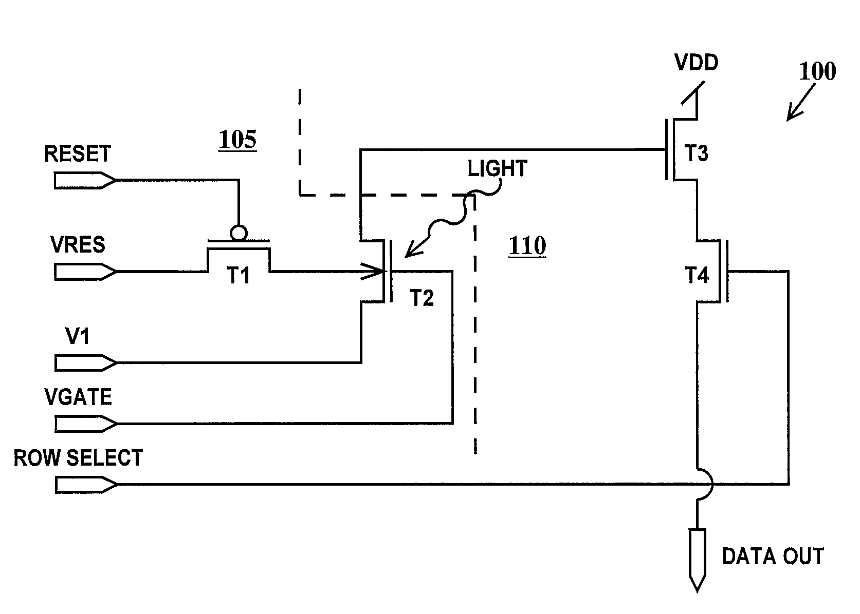
[0019]FIG. 1 is a circuit diagram of a first imaging cell circuit according to the present invention. In FIG. 1, an imaging cell circuit 100 includes a detector section 105 and a read out section 110. Detector section 105 includes a reset PFET T1 and a collection NFET T2. Read out section 110 includes NFETs T3 and T4. The drain of PFET T1 is connected to a VRES pin. The VRES pin is connected to a reset voltage supply. The reset voltage level may be ground or some other starting bias voltage for the well. The gate of PFET T1 is connected to a RESET pin, and the source of PFET T1 is connected to the body of NFET T2. The drain of NFET T2 is connected to a V1 pin, the gate of NFET T2 is connected to a VGATE pin and the source of NFET T2 is connected to the gate of NFET T3. NFET T3 is a source follower. The drain of NFET T3 is connected to a voltage source VDD and the source of NFET T3 is connected to the drain of NFET T4. The gate of NFET T4 is connected to a ROW SELECT pin and the sour...


PUM


Abstract

An imaging circuit, an imaging sensor, and a method of imaging. The imaging cell circuit including one or more imaging cell circuits, each imaging cell circuit comprising: a transistor having a floating body for holding charge generated in the floating body in response to exposure of the floating body to electromagnetic radiation; means for biasing the transistor wherein an output of the transistor is responsive to the electromagnetic radiation; and means for selectively connecting the floating body to a reset voltage supply.

Description

[0001] This application is a division if copending application Ser. No. 10 / 906,625 filed on Feb. 28, 2005.FIELD OF THE INVENTION [0002] The present invention relates to the field of solid-state imagers; more specifically, it relates to a body potential imaging cell and array. BACKGROUND OF THE INVENTION [0003] Imaging sensors are well known in the art. Imaging sensors are used in cameras and other detectors to provide an image of a scene or object for display or output purposes. Imaging sensors are operative over various sections of the electromagnetic spectrum and at various intensity levels. Imaging sensors operate by converting electromagnetic energy to charge. The charge is collected and is sensed by an output device. Typically, the charge is collected on a capacitor and the voltage of the capacitor is sensed. Devices using these imaging arrays have relatively slow shutter speeds, low contrast and high power consumption. [0004] Therefore, there is a need for an imaging cell with...

Claims


Application Information

Patent Timeline
Patent Type & Authority Applications(United States)
IPC IPC(8): H01L31/0352
CPCH01L27/14603H01L27/14679H01L27/14643H01L27/14609
Inventor ELLIS-MONAGHAN, JOHN J.JAFFE, MARK D.LOISEAU, ALAIN
Owner GLOBALFOUNDRIES INC
Features
  • Generate Ideas
  • Intellectual Property
  • Life Sciences
  • Materials
  • Tech Scout
  • Unparalleled Data Quality
  • Higher Quality Content
  • 60% Fewer Hallucinations
Learn More