Biometric sensor and sensor panel

a biometric sensor and sensor panel technology, applied in the field of biometric sensors, can solve the problems of inability to meet the needs of small portable devices with limited computational capacity, inability to use capacitive fingerprint sensors, theft and misappropriation of identity information, etc., and achieve the effects of reducing the number of microprocessors, and improving the accuracy of microprocessors

Inactive Publication Date: 2008-03-06
IVI HLDG
View PDF3 Cites 154 Cited by
  • Summary
  • Abstract
  • Description
  • Claims
  • Application Information

AI Technical Summary

Problems solved by technology

For example, “ID-based fraud” includes such items as improper payment card usage, theft and misappropriation of identity information and even the use of false credentials.
However, such capacitive fingerprint sensors are typically affected by the condition of a finger, such as moisture and / or dirt on the finger.
However, optical fingerprint sensors typically require complex detection circuitry and extensive data processing for pattern recognition, they are not suitable for small portable devices with limited computational capacity, or “card” applications such as smart cards, credit cards, bank cards, driver's licenses, passports, and the like.
For example, the cost of conventional fingerprint sensors including a sensor array using standard CMOS technology would make it economically impractical at the present time to be implemented in such card applications.

Method used


Image

  • Biometric sensor and sensor panel
  • Biometric sensor and sensor panel
  • Biometric sensor and sensor panel

Examples


Embodiment Construction

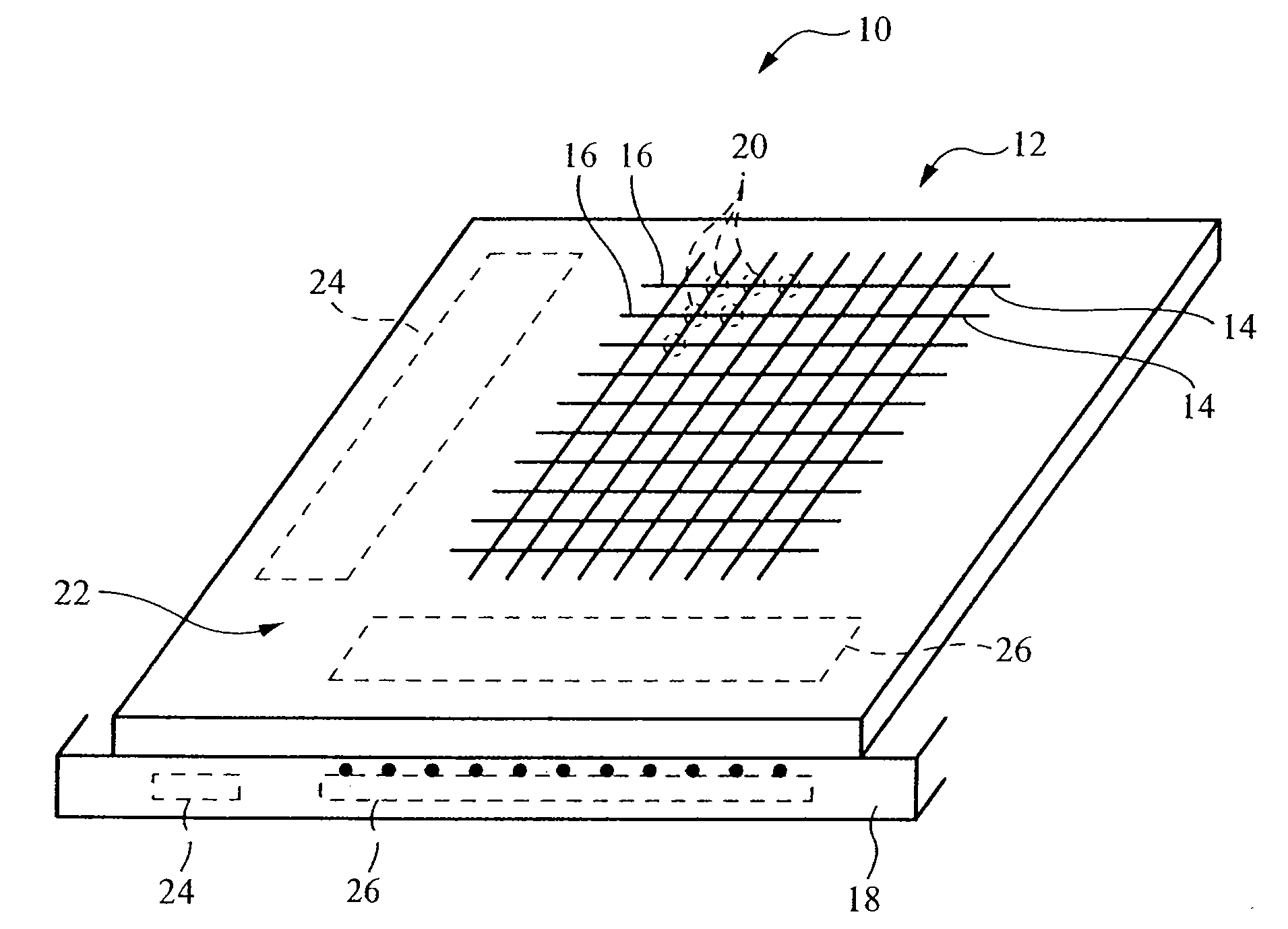
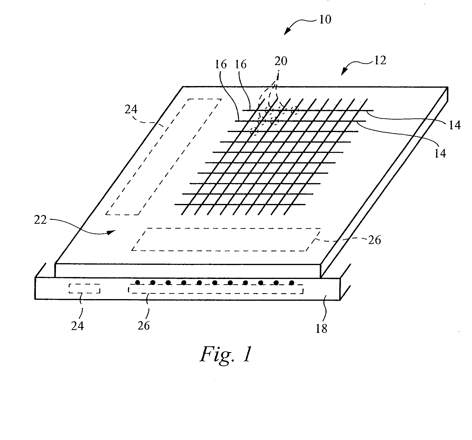
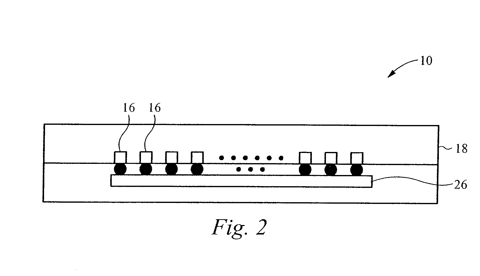
[0048]Embodiments of the present invention are described herein in the context of a biometric sensor, a sensor panel, a method for detecting a biometric pattern using the same, and method for manufacturing the same. Those of ordinary skill in the art will realize that the following detailed description of the present invention is illustrative only and is not intended to be in any way limiting. Other embodiments of the present invention will readily suggest themselves to such skilled persons having the benefit of this disclosure. Reference will now be made in detail to implementations of the present invention as illustrated in the accompanying drawings.

[0049]In the interest of clarity, not all of the routine features of the implementations described herein are shown and described. It will, of course, be appreciated that in the development of any such actual implementation, numerous implementation-specific decisions must be made in order to achieve the developer's specific goals, such...


PUM

PropertyMeasurementUnit
widthaaaaaaaaaa
widthaaaaaaaaaa
widthaaaaaaaaaa

Abstract

A biometric sensor panel includes (a) a first flexible substrate, (b) a plurality of first electrodes formed on the first flexible substrate, the first electrodes being arranged in a first direction, (c) a semiconductor layer formed on the first electrodes, (d) a second flexible substrate, (e) a plurality of second electrodes formed on the second flexible substrate, the second electrodes being arranged in a second direction crossing the first direction, and (f) a pressure sensitive conductive layer formed on the second electrodes, wherein the first and second flexible substrates face each other such that the semiconductor layer is in contact with the pressure sensitive conductive layer.

Description

CROSS-REFERENCES TO RELATED APPLICATIONS[0001]This application is related to U.S. Provisional Patent Application No. 60 / 731,385 (Attorney Docket No. 026893-001300US), entitled “Biometric Sensor, Method for Detecting Biometric Pattern Using The Same, and Method for Manufacturing The Same”, filed on Oct. 28, 2005, and U.S. Provisional Patent Application No. 60 / 759,174 (Attorney Docket No. 026893-001400US), entitled “Biometric Sensor, Method for Detecting Biometric Pattern Using The Same, and Method for Manufacturing The Same”, filed on Jan. 13, 2006, the entire disclosures of these applications are incorporated herein by reference for all purposes.FIELD OF THE INVENTION[0002]The present invention relates to biometric sensors. More particularly, the present invention relates to a biometric sensor and sensor panel, a method for detecting a biometric pattern using the biometric sensor panel, and a method for manufacturing the biometric sensor and sensor panel.BACKGROUND OF THE INVENTION[...

Claims


Application Information

Patent Timeline
Patent Type & Authority Applications(United States)
IPC IPC(8): G06K9/62G01L1/04
CPCA61B5/1172G06K9/0002G01L1/205G06V40/1306
Inventor SAITO, TAMIO
Owner IVI HLDG
Why Eureka
Try Eureka