
Active matrix display apparatus and electronic apparatus

a technology of active matrix and electronic equipment, which is applied in the direction of electrical equipment, semiconductor devices, instruments, etc., can solve the problems of large amount of effort required to find the detect portion using a microscope, complex correction processing, and difficult correction processing, so as to reduce the probability of short-circuit defect due to adhesion of contaminant particles, the probability of generating a short-circuit defect due to contaminant particle adhesion is reduced, and the defect is corrected with ease

Inactive Publication Date: 2008-03-13
SONY CORP
View PDF3 Cites 62 Cited by
  • Summary
  • Abstract
  • Description
  • Claims
  • Application Information

AI Technical Summary

Benefits of technology

The present invention provides an active matrix display apparatus that can correct dark spot defects caused by short-circuit defects of organic EL devices. The invention includes a light-emitting device with a simplified structure that includes a single sampling transistor, a single drive transistor, and multiple sub-light-emitting devices. The sub-light-emitting devices are arranged in a matrix and can be separated from the corresponding pixel circuit when a short-circuit defect is generated. This simplifies the correction processing and reduces the complexity of the pixel circuit. The invention also eliminates the need for a redundant structure and simplifies the configuration of each pixel.

Problems solved by technology

In both cases, a laser beam is emitted onto a small area, that is, a short-circuit defect portion, and this makes correction processing difficult.
Furthermore, since such a defect portion is usually small portion, a large amount of effort is necessary to find the detect portion using a microscope.
Moreover, since a laser beam is emitted onto a small area, the correction processing becomes complicated.
The increased number of pixel circuit elements is a significant factor of difficulty in production of a high-resolution panel.
Accordingly, the technique of the related art has a disadvantage that makes production of a high-resolution panel difficult and does not meet the recent strong demand for a high-resolution panel.

Method used


Image

  • Active matrix display apparatus and electronic apparatus
  • Active matrix display apparatus and electronic apparatus
  • Active matrix display apparatus and electronic apparatus

Examples


Embodiment Construction

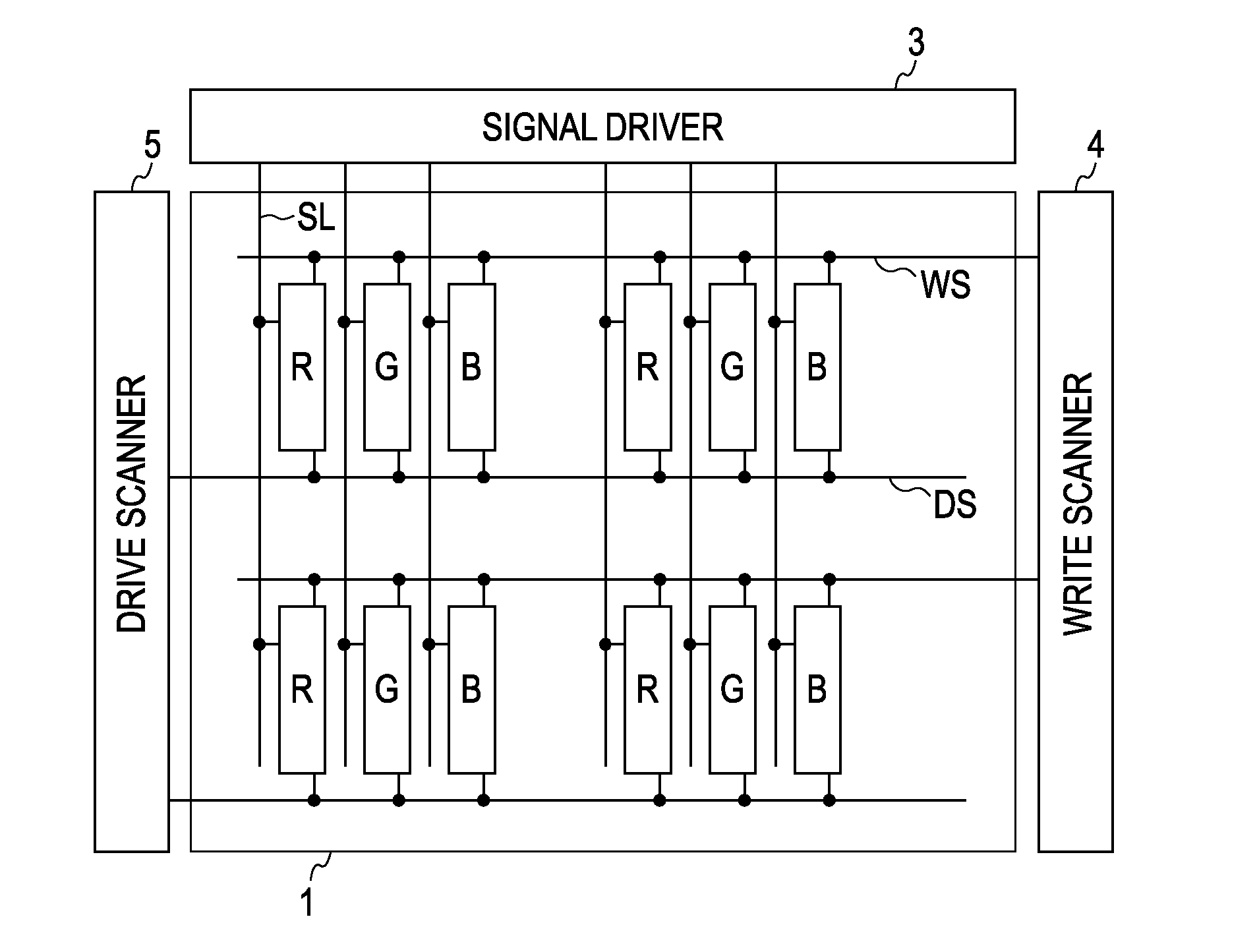
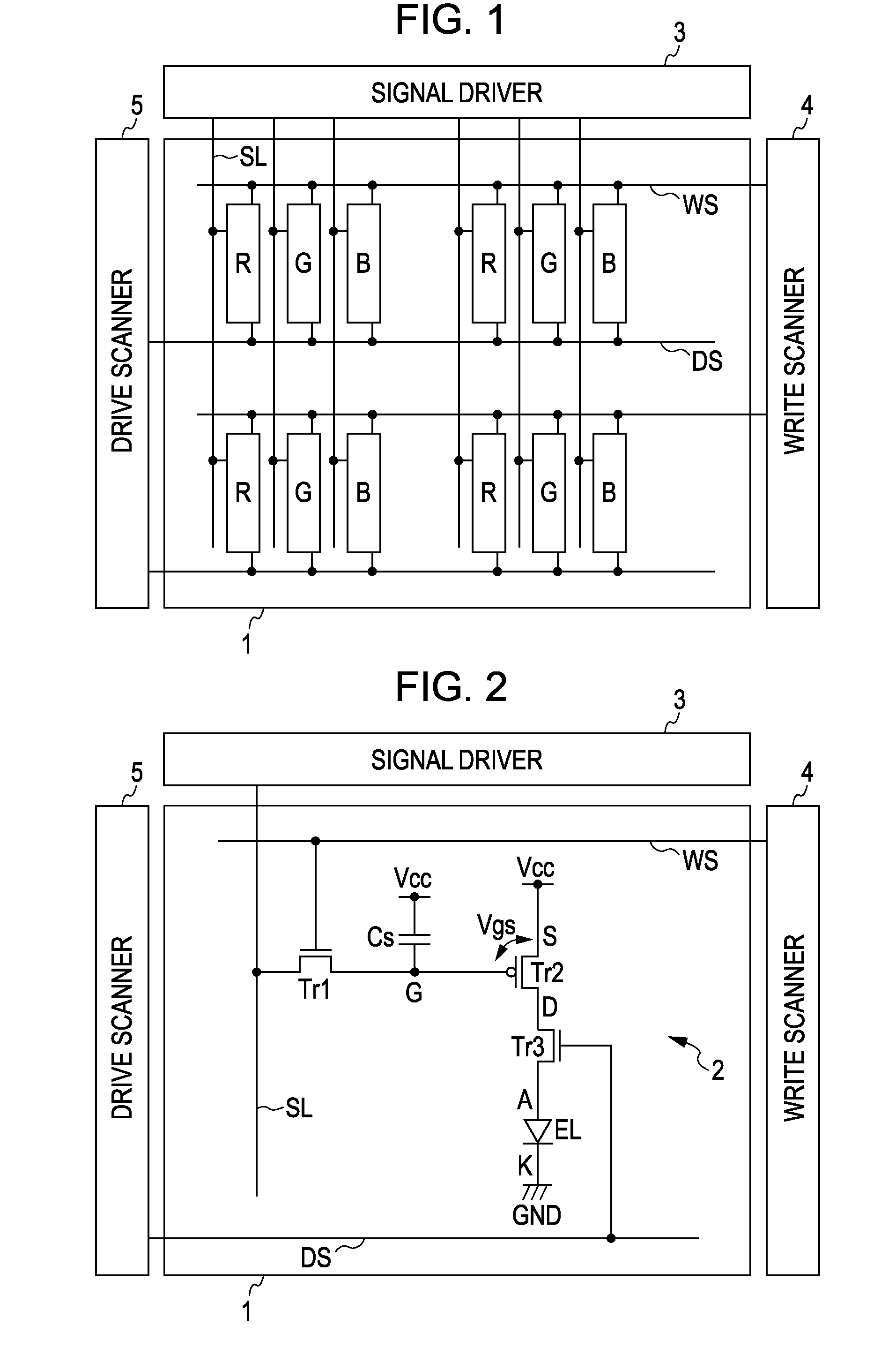
[0040] Embodiments of the present invention will be described hereinafter with reference to the accompanying drawings. FIG. 1 is a block diagram illustrating an entire configuration of an active matrix display apparatus. As shown in FIG. 1, the active matrix display apparatus includes a pixel array portion 1, which is a main portion of the apparatus, and peripheral circuits. The peripheral circuits include a signal driver 3, a write scanner 4, and a drive scanner 5. The pixel array portion 1 includes pixels R, G, and B arranged in a matrix so as to correspond to intersections of scanning lines WS as rows and signal lines SL as columns. Although the pixels R, G, and B are provided for performing color display, the present invention is not limited to this. The signal lines SL are driven by the signal driver 3. The signal driver 3 supplies video signals to the signal lines SL. The scanning lines WS are scanned by the write scanner 4. Note that other scanning lines DS are also arranged ...


PUM


Abstract

An active matrix display apparatus includes a substrate having scanning lines, signal lines, and pixels thereon. Each of the pixels includes a sampling transistor for taking in a video signal, a drive transistor for generating a driving current, and a light-emitting device which emits light with luminance in accordance with the video signal. The two-terminal thin-film light-emitting device includes an anode and cathode electrodes, and a light-emitting layer arranged therebetween. At least one of the electrodes is divided into pieces whereby the light-emitting device is divided into sub-light-emitting devices. The sub-light-emitting devices receive the driving current from a driving transistor and emit light with luminance in accordance with the video signal. A sub-light-emitting devices including a short-circuit defect is separated from the corresponding one of the pixels and the driving current is supplied to the remaining sub-light-emitting devices, whereby the luminance in accordance with the video signal is maintained.

Description

CROSS REFERENCES TO RELATED APPLICATIONS [0001] The present invention contains subject matter related to Japanese Patent Application JP 2006-244984 filed in the Japanese Patent Office on Sep. 11, 2006, the entire contents of which are incorporated herein by reference. BACKGROUND OF THE INVENTION [0002] 1. Field of the Invention [0003] The present invention relates to active matrix display apparatuses having light-emitting devices such as organic EL devices as pixels, and relates to electronic apparatuses which incorporate such display apparatuses. The present invention specifically relates to a technique of correcting pixels having defects. [0004] 2. Description of the Related Art [0005] In recent years, organic electro-luminescence (EL) display apparatuses have been receiving attention as flat-screen display apparatuses. Since such an organic EL display apparatus uses self-luminous devices as pixels, a wide view angle is achieved and furthermore the need for a backlight may be elim...

Claims


Application Information

Patent Timeline
Patent Type & Authority Applications(United States)
IPC IPC(8): G09G3/32
CPCG09G3/2074G09G3/3233G09G2300/0814G09G2300/0819G09G2300/0842G09G2300/0852H01L2251/568G09G2300/0866G09G2300/0871G09G2310/066G09G2320/045H01L27/3276G09G2300/0861H10K59/131H10K71/861
Inventor YAMASHITA, JUNICHIUCHINO, KATSUHIDE
Owner SONY CORP
Learn More