Semiconductor integrated circuit

a technology of integrated circuits and semiconductors, applied in the direction of solid-state devices, measurement by measuring electric/magnetic quantity changes, instruments, etc., can solve the problems of increased production costs, change in electric charge leakage of floating gate components,

Inactive Publication Date: 2008-03-27
KK TOSHIBA
View PDF14 Cites 27 Cited by
  • Summary
  • Abstract
  • Description
  • Claims
  • Application Information

AI Technical Summary

Benefits of technology

[0010]A semiconductor integrated circuit according an aspect of the present invention comprises a semiconductor substrate, an element isolation insulating layer formed in a surface region of the semiconductor substrate, and first and second MIS type devices isolated from each other by the element isolation insulating layer and formed in adjacent first and second element regions in

Problems solved by technology

However, electric charge leakage from the floating gate changes depending on a manufacturing fluctuation.
Since this means that a

Method used


Image

  • Semiconductor integrated circuit
  • Semiconductor integrated circuit
  • Semiconductor integrated circuit

Examples


first embodiment

(2) First Embodiment

[0089]A. Structure

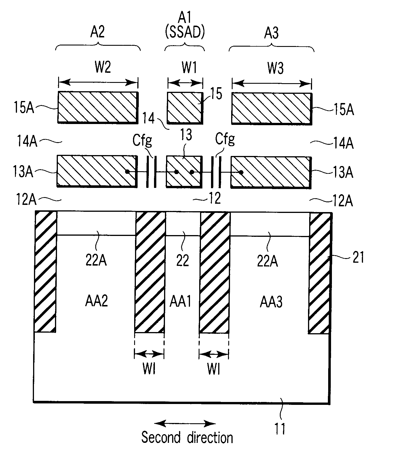
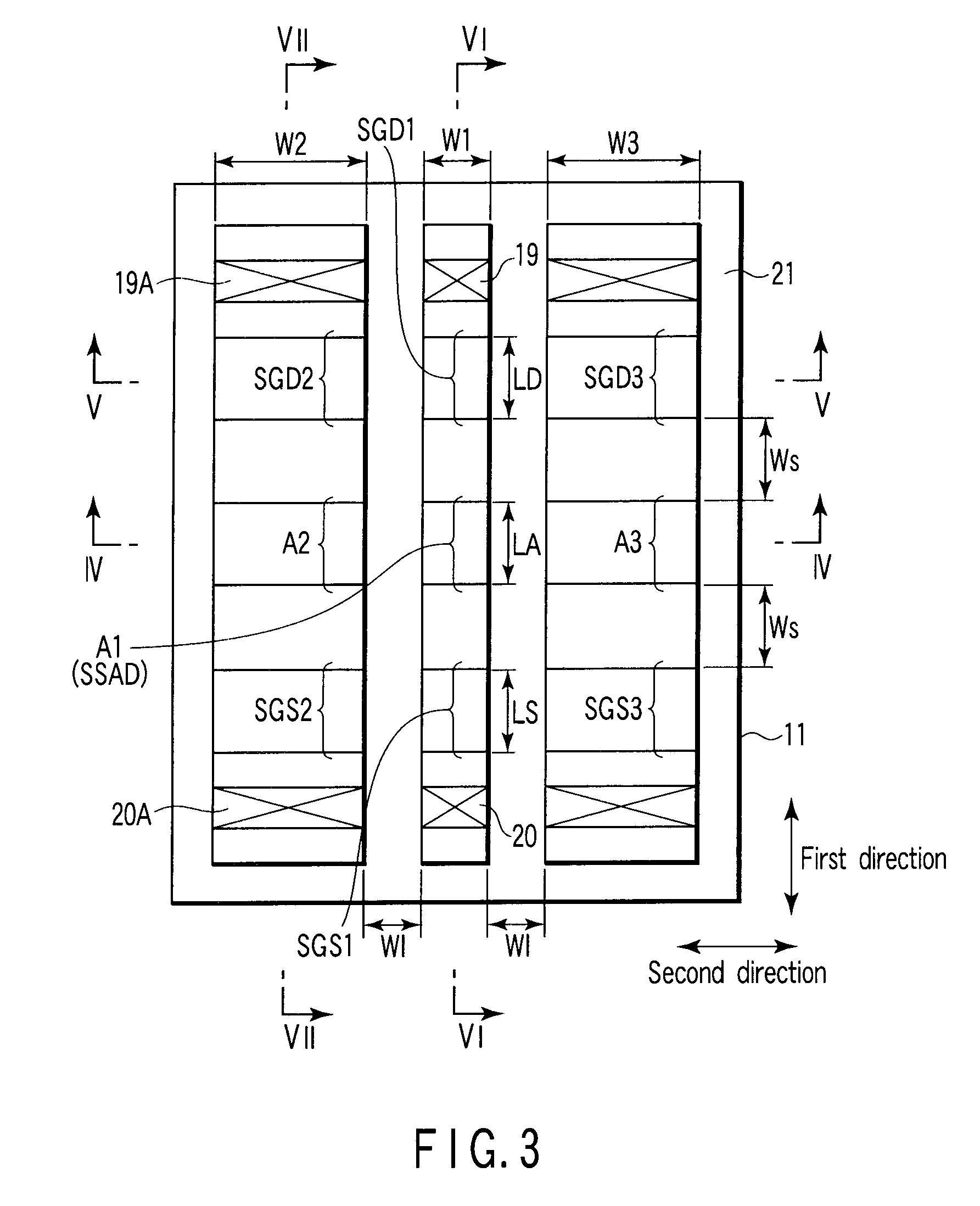
[0090]FIG. 3 shows a plan view of a semiconductor integrated circuit according to a first embodiment.

[0091]FIG. 4 is a sectional view along the IV-IV line in FIG. 3, FIG. 5 is a sectional view along the V-V line in FIG. 3, FIG. 6 is a sectional view along the VI-VI line in FIG. 3, and FIG. 7 is a sectional view along the VII-VII line in FIG. 3.

[0092]In a semiconductor substrate 11, an element isolation insulating layer 21 having an STI (shallow trench isolation) structure is formed. First, second, and third element regions (active areas) AA1, AA2, and AA3 are isolated from each other by the element isolation insulating layer 21 and adjacently arranged in a second direction orthogonal to a first direction.

[0093]A width W1 in the second direction of the first element region AA1 is laid out to be smaller than widths W2 and W3 in the second direction of the second and third element regions AA2 and AA3.

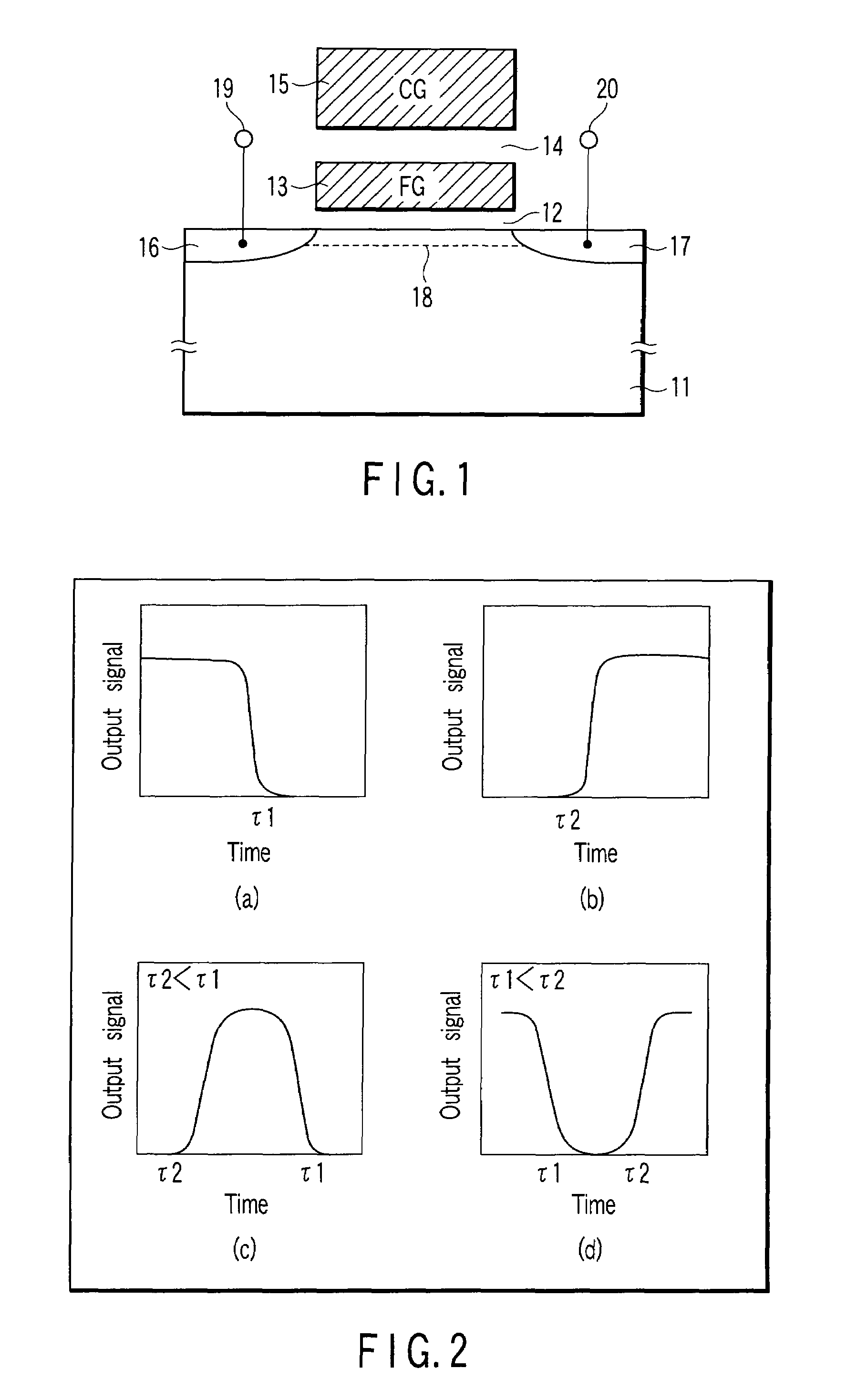
[0094]In the first element region AA1, a first M...

second embodiment

(2) Second Embodiment

[0200]A. Structure

[0201]FIG. 20 is a plan view of a semiconductor integrated circuit according to a second embodiment.

[0202]FIG. 21 is a sectional view along the XIX-XIX line in FIG. 20, FIG. 22 is a sectional view along the XX-XX line in FIG. 20, and FIG. 23 is a sectional view along the XXI-XXI line in FIG. 20.

[0203]In the first embodiment, an array of the control device, the aging device, and the control device arranged in the order named is formed through the element isolation insulating layer. However, in the second embodiment, an array of a control device, an aging device, and a control device arranged in the order named is formed in one element region.

[0204]In the semiconductor substrate 11, an element isolation insulating layer 21 having an STI structure is formed. An element region (active area) AA is surrounded by the element isolation insulating layer 21. The width of the element region (active area) AA in the second direction is set as W1.

[0205]In th...

third embodiment

(4) Third Embodiment

[0246]A third embodiment is a modification of the first embodiment.

[0247]In order to improve the performance of an aging device, interference between the aging device and the control device is preferably increased, and interference between the aging device and the select gate transistor is preferably decreased.

[0248]In the first embodiment, as one of means for this purpose, as shown in FIG. 29, the width of the floating gate of the first MIS type device A1 serving as the aging device in a first direction is larger than the width thereof in the second direction.

[0249]In contrast to this, in the third embodiment, dents on both the sides of a floating gate of an aging device in a first direction are provided to increase the interference between the aging device and the control device and to decrease the interference between the aging device and the select gate transistor.

[0250]A. Structure

[0251]FIG. 30 shows a plan view of a semiconductor integrated circuit accordin...


PUM


Abstract

A semiconductor integrated circuit according to an example of the present invention includes a semiconductor substrate, an element isolation insulating layer formed in a surface region of the semiconductor substrate, and first and second MIS type devices isolated from each other by the element isolation insulating layer and formed in adjacent first and second element regions in a second direction orthogonal to a first direction. Each of the first and second MIS type devices has a stack gate structure having a floating gate and a control gate electrode. The first MIS type device functions as an aging device, and the second MIS type device functions as a control device which controls an electric charge retention characteristic of the aging device.

Description

CROSS-REFERENCE TO RELATED APPLICATIONS[0001]This application is based upon and claims the benefit of priority from prior Japanese Patent Applications No. 2006-257752, filed Sep. 22, 2006; and No. 2007-186344, filed Jul. 17, 2007, the entire contents of both of which are incorporated herein by reference.BACKGROUND OF THE INVENTION[0002]1. Field of the Invention[0003]The present invention relates to a semiconductor integrated circuit having an electronic timer being free from a battery.[0004]2. Description of the Related Art[0005]In recent years, an electronic timer being free from a battery, i.e., an aging device the output of which changes with elapsed time begins to be considered to be used in fields of contents distribution, credit cards, rental digital products, rental digital software, and the like.[0006]The aging device has a stack gate structure constituted by a floating gate and a control gate electrode and functions as an electronic timer which measures a predetermined peri...

Claims


Application Information

Patent Timeline
IPC IPC(8): H01L29/788
CPCG04F10/10G04F13/00G11C16/0433H01L27/11524H01L27/115H01L27/11521H01L21/28273H01L29/40114H10B69/00H10B41/30H10B41/35
Inventor WATANABE, HIROSHINISHIYAMA, AKIRA
Owner KK TOSHIBA
Why Eureka
Try Eureka