Solid-state imaging device, method of manufacturing solid-state imaging device, and electronic apparatus

a solid-state imaging and imaging device technology, applied in the direction of radio frequency controlled devices, transistors, television systems, etc., can solve the problems of increased noise and distortion in captured images, and achieve the effect of suppressing nois

Inactive Publication Date: 2011-10-13
SONY CORP
View PDF3 Cites 47 Cited by
  • Summary
  • Abstract
  • Description
  • Claims
  • Application Information

AI Technical Summary

Benefits of technology

[0024]According to the first to ninth embodiments of the invention, it is possible to more effectively suppress noise.

Problems solved by technology

However, in the CMOS image sensor, since the read operation is performed for each row of the pixel array, the accumulation periods of the signal charges in all the pixels are not coincident with each other, and in the case were a subject is moved, distortion occurs in a captured image.
Therefore, the electrons generated in the weak electric field area through the photoelectric conversion are diffused toward the side of the memory portion with high probability, so that the noise is increased.

Method used


Image

  • Solid-state imaging device, method of manufacturing solid-state imaging device, and electronic apparatus
  • Solid-state imaging device, method of manufacturing solid-state imaging device, and electronic apparatus
  • Solid-state imaging device, method of manufacturing solid-state imaging device, and electronic apparatus

Examples


Embodiment Construction

[0043]Hereinafter, specific embodiments of the invention will be described in detail with reference to the drawings.

[0044]FIG. 1 is a block diagram illustrating an example of a configuration of a solid-state imaging device according to an embodiment of the invention.

[Example of Configuration of Solid-State Imaging Device]

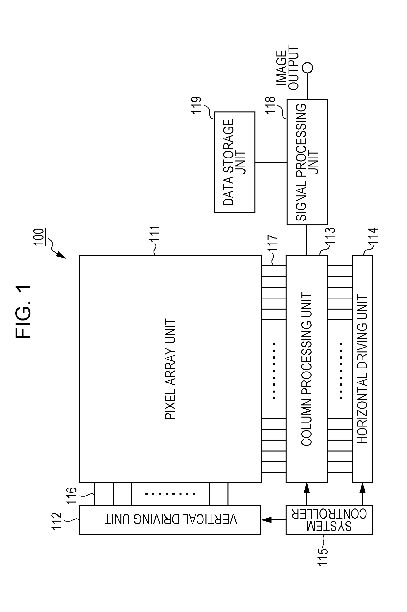
[0045]FIG. 1 is a block diagram illustrating an example of a configuration of a CMOS image sensor as a solid-state imaging device according to an embodiment of the invention.

[0046]The CMOS image sensor 100 is configured to include a pixel array unit 111, a vertical driving unit 112, a column processing unit 113, a horizontal driving unit 114, and a system controller 115. The pixel array unit 111, the vertical driving unit 112, the column processing unit 113, the horizontal driving unit 114, and the system controller 115 are formed on a semiconductor substrate (chip) (not shown).

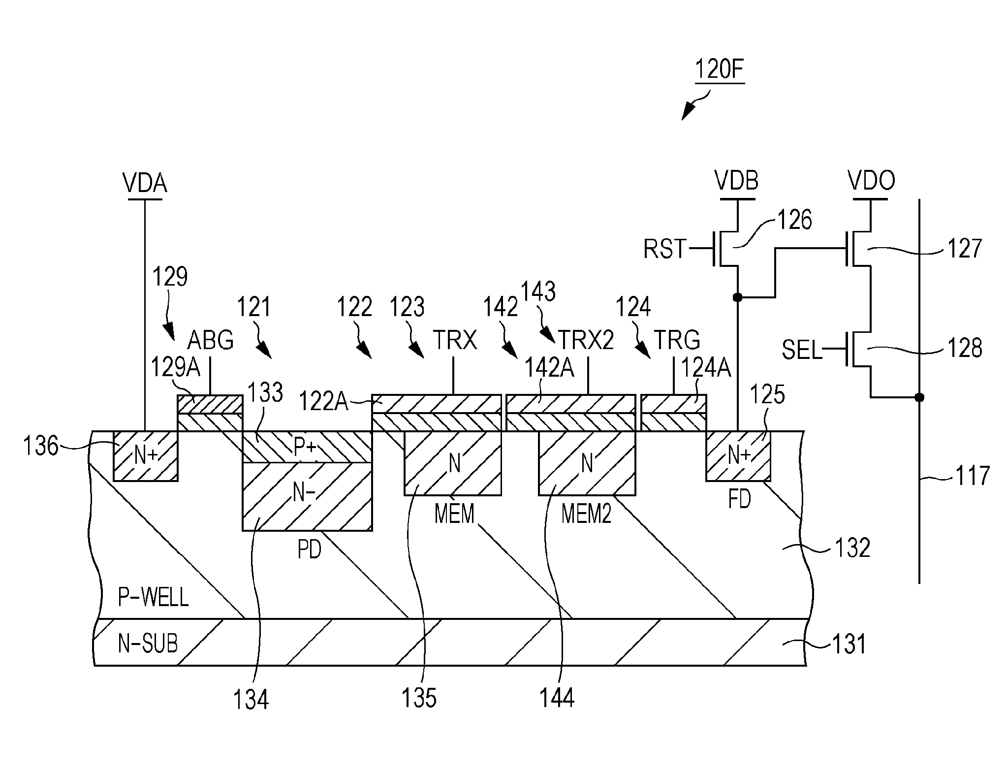
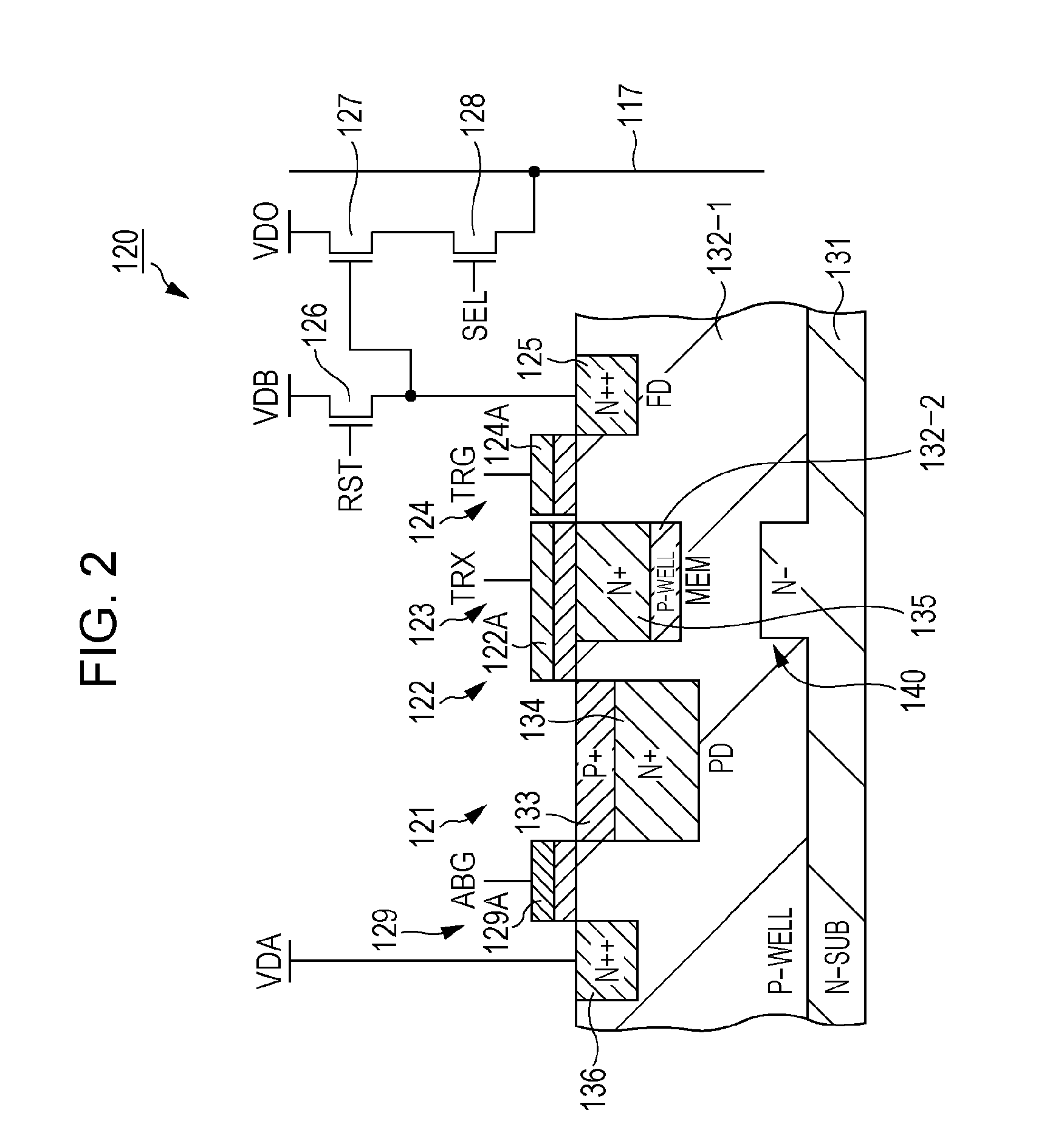
[0047]In the pixel array unit 111, unit pixels (unit pixels 120 of FIG. 2) having photoel...


PUM


Abstract

Provided is a solid-state imaging device including: a first-conductivity-type substrate; a second-conductivity-type well formed in a surface side of the first-conductivity-type substrate; a photoelectric conversion area configured with a first-conductivity-type-impurity area formed in the second-conductivity-type well to convert incident light to charges; a first-conductivity-type-charge retaining area configured with the first-conductivity-type-impurity area formed in the second-conductivity-type well to retain the charges converted by the photoelectric conversion area until the charges are read out; a charge voltage conversion area configured with the first-conductivity-type-impurity area formed in the second-conductivity-type well to convert the charges retained in the charge retaining area to a voltage; and a first-conductivity-type-layer area configured by forming a first-conductivity-type-in a convex shape from a boundary between the first-conductivity-type substrate and the second-conductivity-type well to a predetermined depth of the surface side under at least one portion of the charge retaining area and the charge voltage conversion area.

Description

BACKGROUND OF THE INVENTION[0001]1. Field of the Invention[0002]The invention relates to a solid-state imaging device, a method of manufacturing the solid-state imaging device, and an electronic apparatus, and more particularly to, a solid-state imaging device capable of more effectively suppressing noise, a method of manufacturing the solid-state imaging device, and an electronic apparatus.[0003]2. Description of the Related Art[0004]Recently, in a video camera or an electronic still camera, a CCD (Charge Coupled Device) or a CMOS (Complementary Metal Oxide Semiconductor) image sensor is used as a solid-state imaging device for capturing an image. Particularly, in comparison with the CCD, the CMOS image sensor has excellent characteristics in terms of low power consumption.[0005]In the related art, each pixel included in the CMOS image sensor is configured to include, for example, a photodiode, a transfer gate, a floating diffusion, a reset transistor, an amplification transistor, ...

Claims


Application Information

Patent Timeline
Patent Type & Authority Applications(United States)
IPC IPC(8): H01L27/146H01L31/18
CPCH01L27/14612H01L27/14614H04N5/37452H01L27/14689H04N5/3745H01L27/14656H04N25/77H04N25/771
Inventor MATSUMURA, YUSUKEMACHIDA, TAKASHI
Owner SONY CORP
Why Eureka
Try Eureka