System and method for noise mitigation in high speed printed circuit boards using electromagnetic bandgap structures

Inactive Publication Date: 2005-05-19
UNIV OF MARYLAND
View PDF8 Cites 78 Cited by
  • Summary
  • Abstract
  • Description
  • Claims
  • Application Information

AI Technical Summary

Benefits of technology

[0029] The PCB with the noise suppressing capability may be formed by arranging the HIS stage (or stages) on one of the layers (patch layer) of the multi-layer printed circuit board so that the EEBG structures are connected by the via posts to the conductive plane (power bus or signal layer) on the patch layer of the PCB. The patch layer carrying the EEBG sta

Problems solved by technology

Electromagnetic radiation of high-speed digital and analog circuits is considered one of the most critical challenges to the electromagnetic interference, compatibility and reliability of electronic systems.
The continuous decrease in power supply and threshold voltage levels in CMOS based digital circuits increases their vulnerability to external electromagnetic interference.
Simultaneously, increases in clock and bus speeds increases the potential of the circuit to radiate, thus compromising its compatibility potential and also increasing its security vulnerability.
As the speed of modern high-performance digital circuits rapidly increases, there is a corresponding energy consumption increase.
Although appropriate shielding may generally be achieved, the consequent cost may be significant especially in a number of electronic systems that are cost-sensitive.
Fast switching in digital circuits that use standard printed circuit board (PCB) technology creates simultaneous switching noise (SSN) which is sometimes commonly referred to as ground bounce or Delta-I noise.
Switching noise if left unchecked, may produce several low and high-frequency anomalies.
The most important of these anomalies is the biasing of the power planes that leads to logic errors in digital circuits.
Switching noise is generally caused by the high-speed time-varying currents needed by high-performance digital circuits.
The flow of these currents through vias between layers of a printed circuit boards causes radiation efflux

Method used


Image

  • System and method for noise mitigation in high speed printed circuit boards using electromagnetic bandgap structures
  • System and method for noise mitigation in high speed printed circuit boards using electromagnetic bandgap structures
  • System and method for noise mitigation in high speed printed circuit boards using electromagnetic bandgap structures

Examples


Embodiment Construction

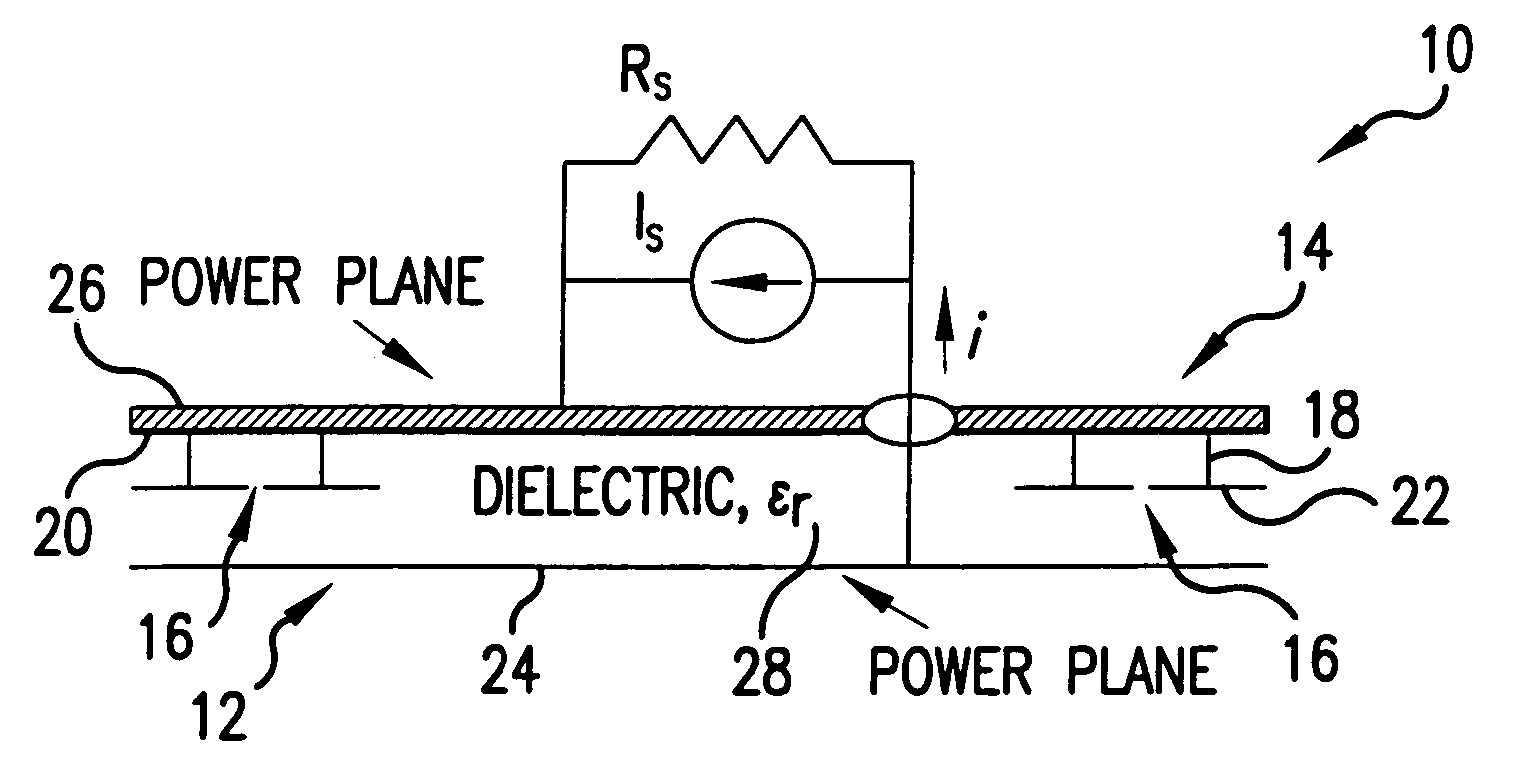
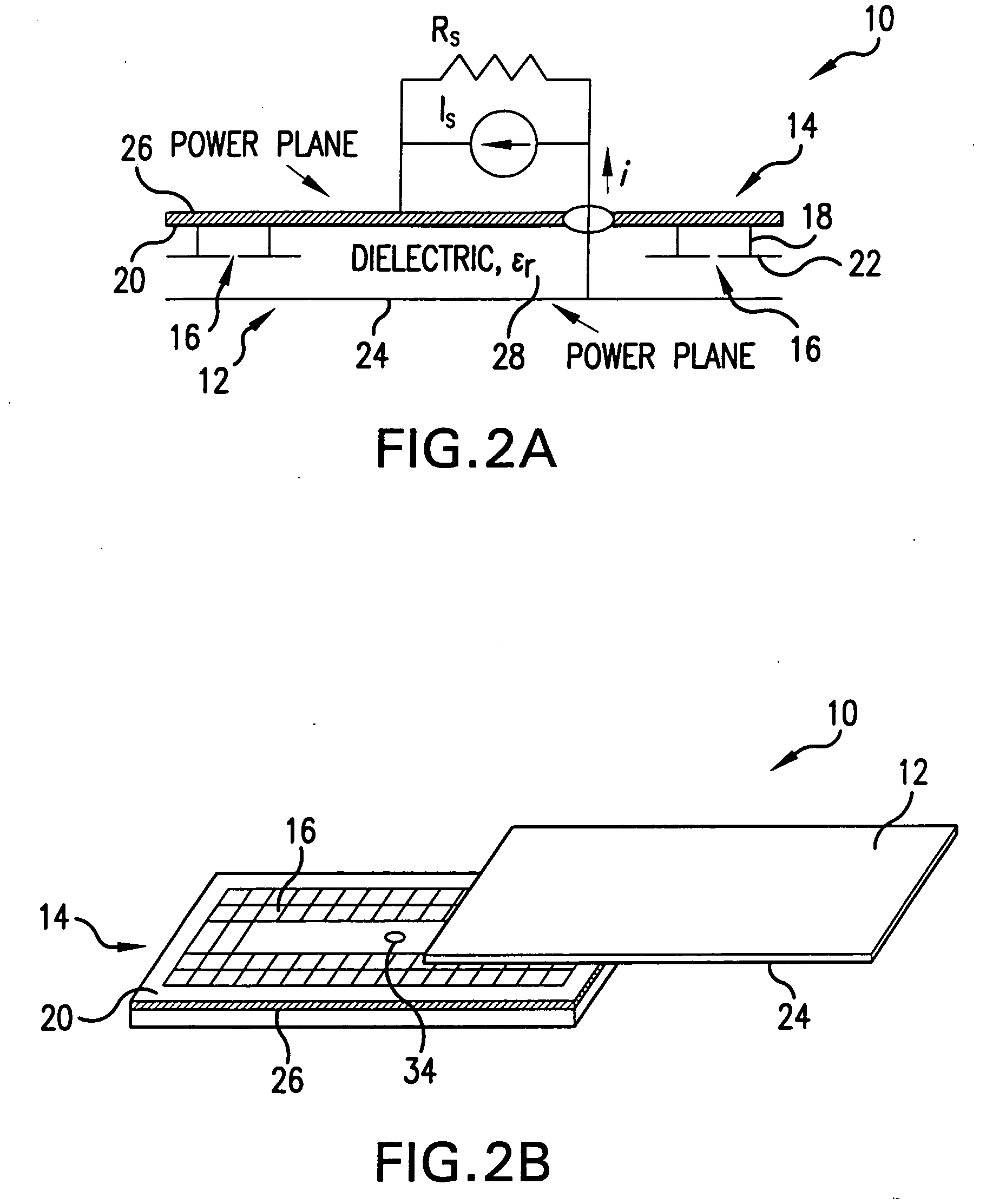
[0048] Referring now to FIGS. 2A and 2B, a multilayer PCB 10 includes a plurality of layers (boards), which can be implemented with commercial PCB technology. The PCB 10 includes boards 12 and 14, which has EBG structure 16 formed thereon which will be further referred to as a “patch layer”14. It will be readily understood by those skilled in the art that the multilayer PCB 10 may include more than two boards. The 2-layer design of FIGS. 2A and 2B is chosen merely for the purpose of simplicity of explanation and not to limit the scope of the present invention. It will be understood by those skilled in the art, that printed circuit boards represent one specific kind of electronic packaging, and the scope of the present invention is not limited to PCBs but is applicable to all electronic packaging methods.

[0049] The Electro-magnetic Band-Gap (EBG) structure 16 is a structure that has an electromagnetic bandgap. The EBG structure 16 is a structure, which as shown in FIGS. 2A, 2B, and ...


PUM


Abstract

Electromagnetic Bandgap (EBG) structures are embedded between adjacent power planes in a multi-layer PCB to decrease the emanation of Electromagnetic radiation induced by power buses, signal layers, as well as to suppress the switching noise. EBG stages with different stop bands are cascaded to create rejection over a wider frequency region. The cascading can be performed in series, or may be formed in a variety of arrangements such as a checkerboard design or concentric ribbons positioned along the perimeter of the PCB. Each EBG stage is composed of conductive patches and via posts extending from each patch, which are positioned at a predetermined distance from each other. By surrounding the source of the noise with EBG stages, a sufficient suppression of electromagnetic noise over specific frequency bands of interest is achieved.

Description

REFERENCE TO RELATED APPLICATIONS [0001] This patent application is based on Provisional Patent Application No. 60 / 502,059 filed Sep. 11, 2003, and Provisional Patent Application No. 60 / 511,843 filed Oct. 16, 2003.FIELD OF THE INVENTION [0002] The present invention relates to suppression of electromagnetic noise. In particular, this invention relates to the mitigation of electromagnetic radiation in electronic packaging, including printed circuit boards (PCBs). [0003] In overall concept, the present invention relates to the application of Electromagnetic Bandgap (EBG) structures for reduction of electromagnetic radiation induced by power buses as well as by signal layers in the printed circuit boards. [0004] The present invention further relates to mitigation of simultaneous switching noises (SSN) in printed circuit boards by embedding EBG structures in the PCBs and more particularly, by cascading EBG stages with different stop bands to attain suppression of the noise over an ultraw...

Claims


Application Information

Patent Timeline
IPC IPC(8): H04B3/28H05K1/00H05K1/02
CPCH05K1/0216H05K1/0298H05K2201/09309H05K2201/09781H05K2201/09609H05K2201/09618H05K2201/09536
Inventor SHAHPARNIA, SHAHROOZRAMAHI, OMAR M.
Owner UNIV OF MARYLAND
Why Eureka
Try Eureka