Schottky Diode Structure with Silicon Mesa and Junction Barrier Schottky Wells

a technology of silicon mesa and diode structure, which is applied in the direction of diodes, semiconductor devices, electrical apparatus, etc., can solve the problems of tanaka failing to realize and the maximum voltage blocking capability of the device being decreased by on-state performance, and achieves high forward conductivity and reverse voltage blocking ability.

Active Publication Date: 2008-08-14
WOLFSPEED INC
View PDF10 Cites 52 Cited by
  • Summary
  • Abstract
  • Description
  • Claims
  • Application Information

AI Technical Summary

Benefits of technology

[0008]In one aspect, the invention is a diode having a silicon mesa atop the drift region. A contact is positioned on the silicon mesa. In a preferred embodiment, the diode has an n− type drift region on which the silicon mesa is formed. The silicon mesa is therefore highly doped p-type (or n-type, depending on the application), and the anode (or cathode) is formed on the mesa. The diode of this invention achieves a high forward conductivity in the on-state and exhibits a significantly higher reverse voltage blocking ability than diodes of the prior art. Under a forward bias, the silicon mesa provides carriers to achieve desirable forward current characteristics. The mesa may be formed of polysilicon. For high reverse voltages (e.g., ≧600 V), p-type polysilicon is desirable. For diodes used in applications with less than 600 V reversed biases, n-type polysilicon is better.
[0009]The diode disclosed herein has superb performance characteristics, even when the substrate is of a significantly reduced thickness. The diode achieves a considerable reverse blocking voltage by implanting junction barrier Schottky wells within the body of the diode, i.e., between the edge of the diode and its absolute center. This allows the diode to support the reverse bias more deeply into the thickness of the drift region.

Problems solved by technology

Buchanan, however, is only concerned with increasing the reverse blocking voltage that the Schottky diode can withstand.
The prior work that incorporates JBS structures in silicon layers fails to solve the problem, however, that increasing on-state performance decreases the maximum voltage blocking capability of the device.
Tanaka fails to realize, however, the possibility of using JBS technology to improve the reverse biased characteristics of the diode by incorporating the JBS implants within the conductive channel of the drift region.

Method used


Image

  • Schottky Diode Structure with Silicon Mesa and Junction Barrier Schottky Wells
  • Schottky Diode Structure with Silicon Mesa and Junction Barrier Schottky Wells
  • Schottky Diode Structure with Silicon Mesa and Junction Barrier Schottky Wells

Examples


Embodiment Construction

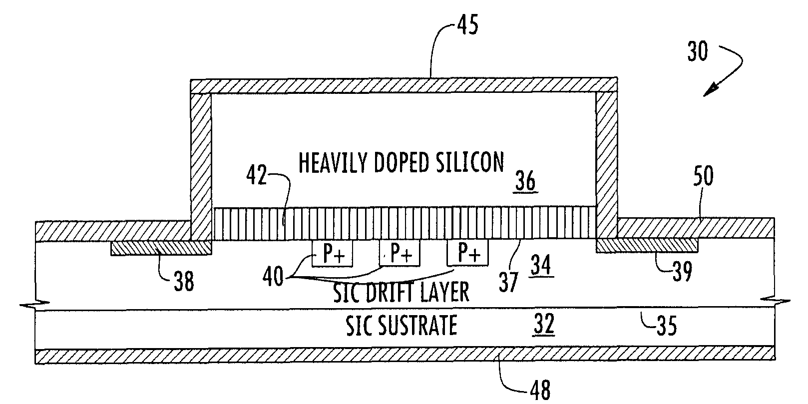
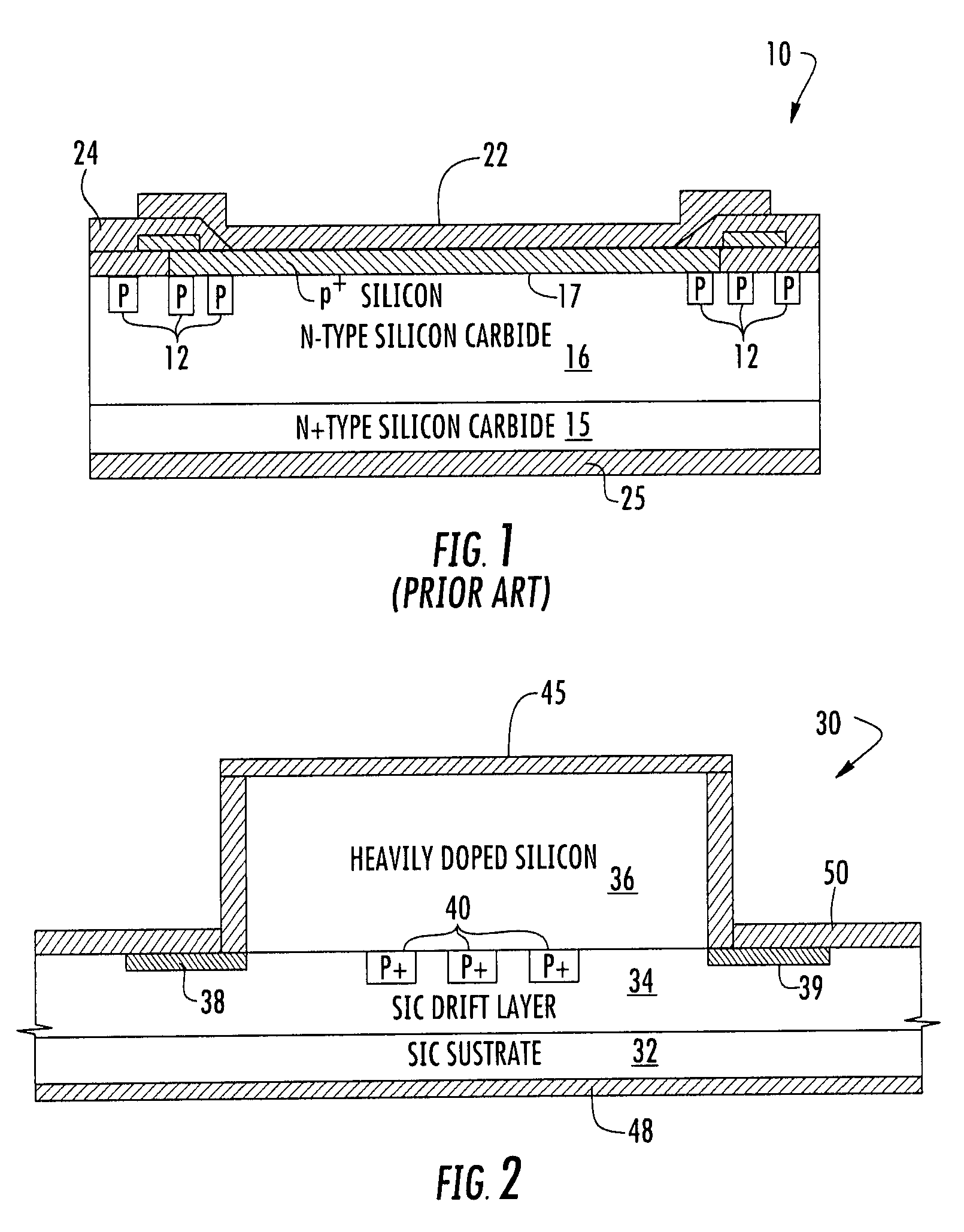
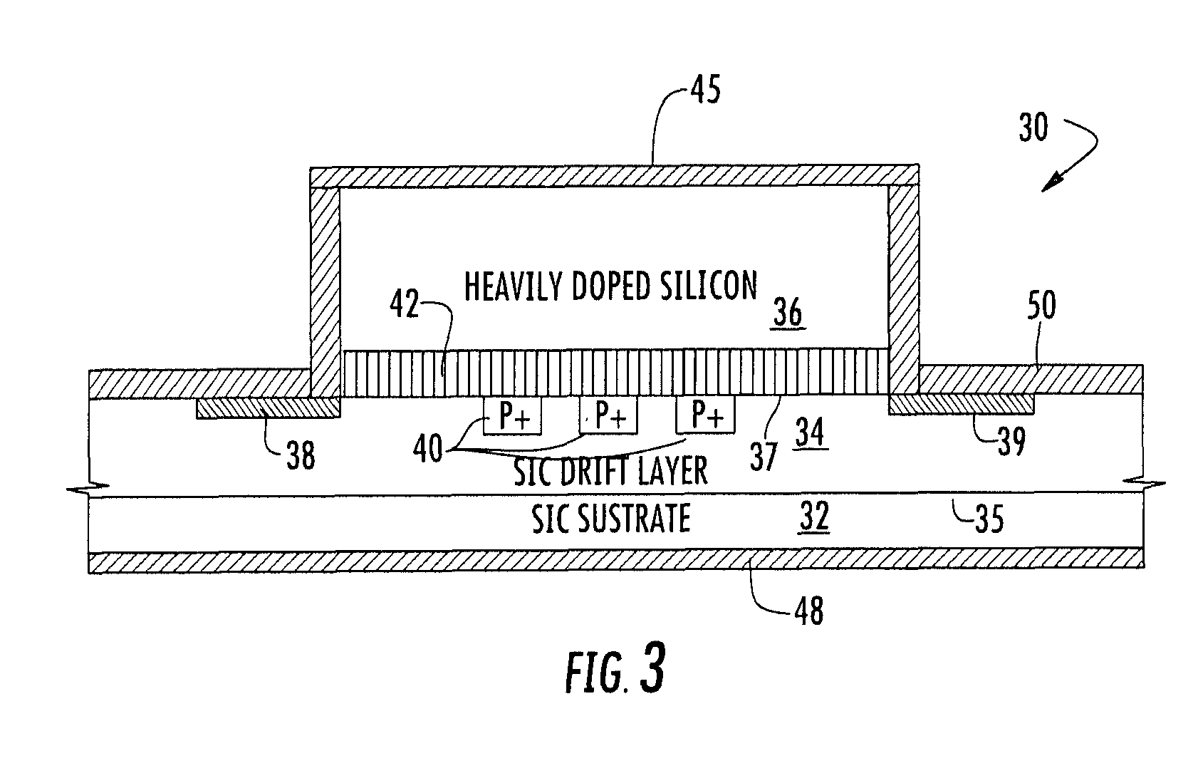
[0018]The diode of this invention achieves a low on-resistance and yields surging capability as well as avalanche breakdown by incorporating a doped silicon mesa and JBS implants into the body of the device. The new construction also allows the substrate to be extremely thin. By adjusting the thickness of the silicon mesa, the diode disclosed herein also maintains sufficient mechanical strength for dicing and incorporating into a larger circuit.

[0019]FIG. 1 shows a prior art heterojunction diode (10) having JBS implants (12) along the edges of the junction region for terminating the device. The diode (10) includes n+ type (15) and n− type (16) silicon carbide layers supporting a p+ type silicon layer (17). The anode (22) is connected to the p+ silicon layer (17), and the edges of the silicon layer (22), the n− layer (16), and the anode (22) are covered with a nonconductive passivation layer (24). The prior art diode (10) is completed with a cathode (25).

[0020]FIG. 2 shows an improve...


PUM


Abstract

A power diode having a silicon mesa atop the drift region includes a first contact positioned on the silicon mesa. The silicon mesa is highly doped p-type or n-type, and the anode may be formed on the mesa. The mesa may include two separate silicon layers, one of which is a Schottky barrier height layer. Under a forward bias, the silicon mesa provides carriers to achieve desirable forward current characteristics. The substrate has a significantly reduced thickness. The diode achieves reverse voltage blocking capability by implanting junction barrier Schottky wells within the body of the diode. The diode utilizes a deeper portion of the drift region to support the reverse bias. The method of forming the diode with a silicon mesa includes forming the mesa within a window on the diode or by thermally or mechanically bonding the silicon layer to the drift region.

Description

BACKGROUND[0001]The present invention relates to the high voltage blocking characteristics of power diodes that also conduct large currents under forward bias. Power diodes are used in multiple applications that require rapid switching between a voltage blocking state that allows no current to pass and an on-state that quickly allows large currents to flow in one direction. The problem addressed in this invention is that of achieving a device that operates optimally in both states.[0002]Current technology includes power Schottky diodes that have doped Junction Barrier Schottky (JBS) structures to improve the blocking characteristics of the diode. Statutory invention registration No. H40 (Buchanan 1986) discloses a silicon power diode that includes field shields within the Schottky barrier of the device. The field shields are highly doped p-type diffusions in the n− type silicon drift layer directly adjacent the metal-silicon heterojunction. Buchanan, however, is only concerned with ...

Claims


Application Information

Patent Timeline
Patent Type & Authority Applications(United States)
IPC IPC(8): H01L27/095
CPCH01L27/0814H01L29/872H01L29/6606H01L29/1608
Inventor ZHANG, QINGCHUNRYU, SEI-HYUNG
Owner WOLFSPEED INC
Why Eureka
Try Eureka