Trench Schottky semiconductor device

A trench type, Schottky potential technology, applied in the direction of semiconductor devices, electrical components, circuits, etc., can solve the problems of limited improvement of device reverse voltage blocking ability, leaving holes, affecting device reliability, etc., to achieve enhanced Effects of reverse voltage blocking capability, increased directional blocking voltage, and improved reliability

Active Publication Date: 2017-05-10
SUZHOU SILIKRON SEMICON CO LTD
View PDF7 Cites 0 Cited by
  • Summary
  • Abstract
  • Description
  • Claims
  • Application Information

AI Technical Summary

Problems solved by technology

[0005] However, the main problem exposed by this structural design is the limited improvement of the reverse voltage blocking capability of the device.
like figure 2 As shown in the electric field strength curve in the figure, the position of the peak value of the electric field strength changes with the depth of the trench, but the area surrounded by the electric field strength curve does not change significantly, that is, the reverse voltage blocking capability of the device does not change significantly.
In addition, the metal filled in the trench is the same as that of the upper metal layer. When the width of the trench is narrow, due to the poor gap filling ability of the upper metal layer material, voids may be left, which will affect the reliability of the device.

Method used


Image

  • Trench Schottky semiconductor device
  • Trench Schottky semiconductor device
  • Trench Schottky semiconductor device

Examples


Embodiment

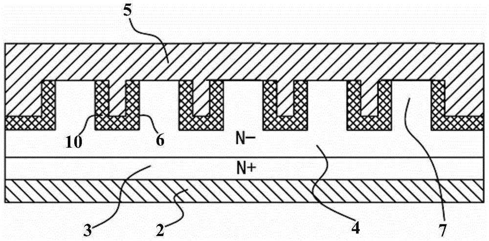
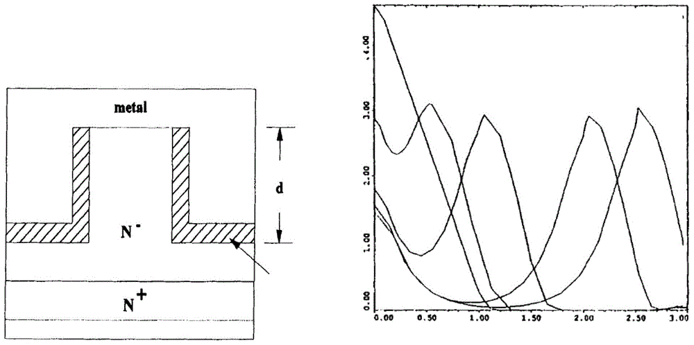
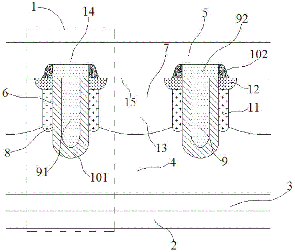
[0022] Embodiment: A trench-type Schottky semiconductor device. On a top plane, the active area of ​​the device is composed of a plurality of Schottky barrier diode cells 1 in parallel, and this Schottky barrier diode cell 1 In the longitudinal section, each Schottky barrier diode unit cell 1 includes a lower metal layer 2 on the back side of the silicon wafer, and a heavily doped substrate layer 3 of the first conductivity type above the lower metal layer 2. An ohmic contact is formed with the lower metal layer 2, a lightly doped epitaxial layer 4 of the first conductivity type is provided above the substrate layer 3, and an upper metal layer 5 and a trench 6 are provided above the epitaxial layer 4 From the upper surface of the epitaxial layer 4 and extending to the middle of the epitaxial layer 4, the area of ​​the epitaxial layer 4 between adjacent trenches 6 forms a monocrystalline silicon boss 7 of the first conductivity type, and the top surface of the monocrystalline sil...


PUM


Abstract

The invention discloses a groove type schottky semiconductor device. In the device, a conductive polycrystalline silicon body is embedded in a bar groove, wherein a polycrystalline silicon middle lower part positioned at the middle lower part of the conductive polycrystalline silicon body is positioned in the bar groove; a first silicon oxide oxidation layer is arranged between an epitaxial layer and the polycrystalline silicon middle lower part; a second conductive type doping area is positioned in a polycrystalline silicon lug boss and arranged on the side surfaces of the periphery of the groove; a heavy doping second conductive type doping area is arranged between the top of the second conductive type doping area and the upper surface of the epitaxial layer; an epitaxial divided layer having the first conductive type is positioned between respective second conductive type doping areas of adjacent schottky barrier diode unit cells; the depth of the epitaxial divided layer is smaller than that of the second conductive type doping area; positioned at the upper part of the epitaxial layer, the doping density of the epitaxial divided layer is larger than that of the epitaxial layer. According to the invention, the reliability of the device is improved, the electric potential is reduced at the top of the groove, the forward voltage drop and loss of the device are reduced, and moreover, when the device is cut off reversely, the electric leakage of the device is further reduced.

Description

Technical field [0001] The invention relates to a rectifier device, in particular to a trench-type Schottky semiconductor device. Background technique [0002] Schottky barrier diodes have been used in power applications for decades as rectifier devices. Compared with PN junction diodes, Schottky barrier diodes have the advantages of low forward turn-on voltage and fast switching speed, which makes them very suitable for switching power supplies and high-frequency applications. The reverse recovery time of the Schottky barrier diode is very short, which is mainly determined by the parasitic capacitance of the device, not by the minority carrier recombination time like the PN junction diode. Therefore, the Schottky barrier diode rectifier device can effectively reduce the switching power loss. [0003] Schottky barrier diodes are made using the principle of a metal-semiconductor junction formed by contact between metal and semiconductor. The traditional planar Schottky barrier di...

Claims


Application Information

Patent Timeline
Patent Type & Authority Patents(China)
IPC IPC(8): H01L29/872H01L29/06
CPCH01L29/0619H01L29/8725
Inventor 徐吉程毛振东薛璐
Owner SUZHOU SILIKRON SEMICON CO LTD
Why Eureka
Try Eureka