Enhanced grooved Schottky diode rectification device and fabrication method thereof

A technology of Schottky diodes and rectifier devices, which is applied in semiconductor/solid-state device manufacturing, semiconductor devices, electrical components, etc. It can solve the problems of limited improvement of device reverse voltage blocking ability, leaving holes, affecting device reliability, etc. , to achieve the effect of enhancing the reverse voltage blocking ability and strong gap filling ability

Inactive Publication Date: 2014-11-05
SUZHOU SILIKRON SEMICON CO LTD
View PDF5 Cites 9 Cited by
  • Summary
  • Abstract
  • Description
  • Claims
  • Application Information

AI Technical Summary

Problems solved by technology

[0004] However, the main problem exposed by this structural design is the limited improvement of the reverse voltage blocking capability of the device.
like figure 2 As shown in the electric field strength curve in the figure, the position of the peak value of the electric field strength changes with the depth of the trench, but the area surrounded by the electric field strength curve does not change significantly, that is, the reverse voltage blocking capability of the device does not change significantly.
In addition, the metal filled in the trench is the same as that of the upper metal layer. When the width of the trench is narrow, due to the poor gap filling ability of the upper metal layer material, voids may be left, which will affect the reliability of the device.

Method used


Image

  • Enhanced grooved Schottky diode rectification device and fabrication method thereof
  • Enhanced grooved Schottky diode rectification device and fabrication method thereof
  • Enhanced grooved Schottky diode rectification device and fabrication method thereof

Examples


Embodiment

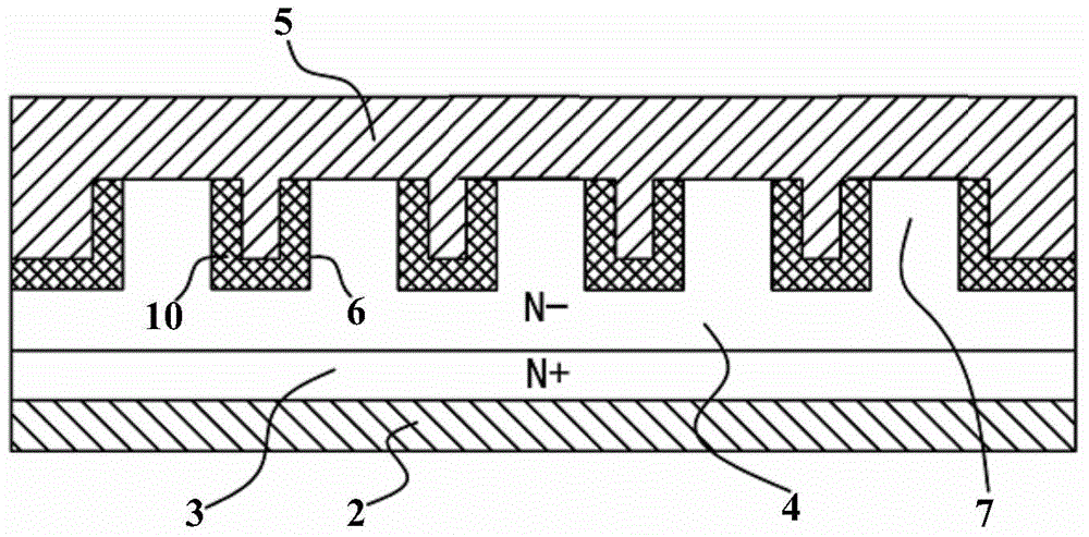
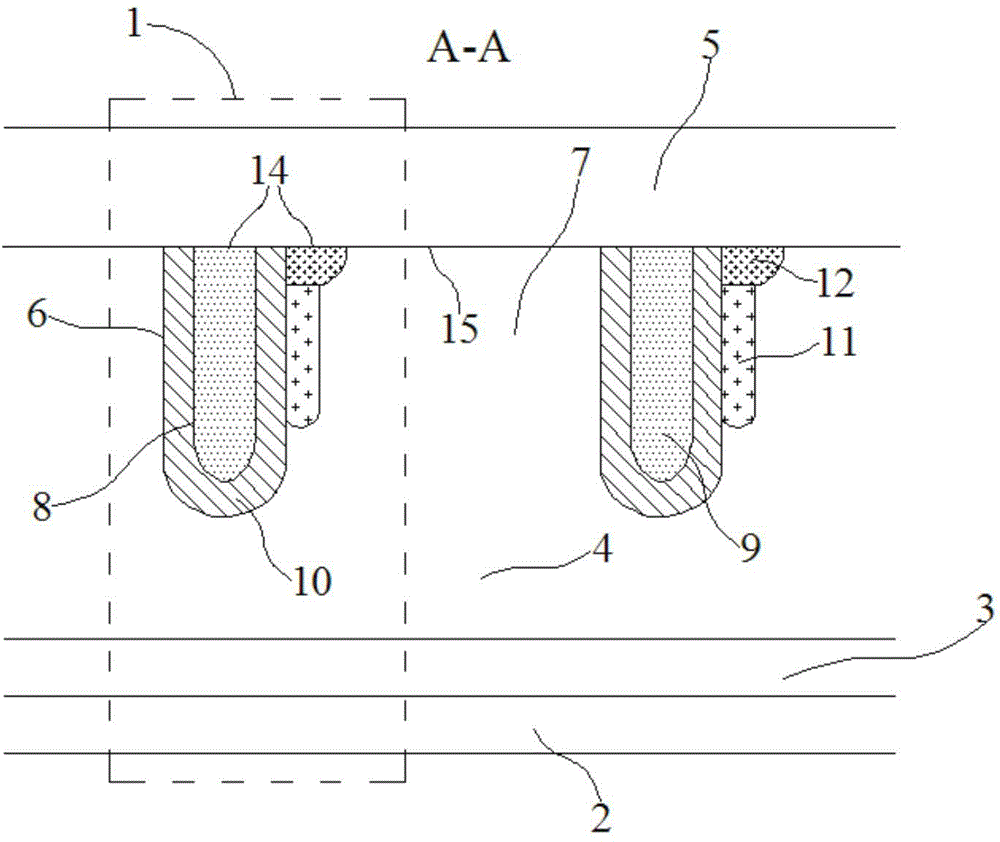
[0038] Embodiment: an enhanced trench type Schottky diode rectifier device, on the top view plane, the active region of the device is composed of several Schottky barrier diode cells 1 connected in parallel, the Schottky barrier diode In the longitudinal section of the unit cell 1, each Schottky barrier diode unit cell 1 includes a lower metal layer 2 located on the back of the silicon wafer, and a substrate layer 3 heavily doped with the first conductivity type located above the lower metal layer 2. An ohmic contact is formed between the substrate layer 3 and the lower metal layer 2, an epitaxial layer 4 lightly doped with the first conductivity type located above the substrate layer 3, and an upper metal layer 5 located above the epitaxial layer 4, from the epitaxial The upper surface of the layer 4 extends to the groove 6 in the middle of the epitaxial layer 4, and the region of the epitaxial layer 4 between adjacent grooves 6 forms a single crystal silicon boss 7 of the fir...


PUM


Abstract

The invention discloses an enhanced grooved Schottky diode rectification device. Grooves extend from the upper surface of an epitaxial layer to a middle part of the epitaxial layer, a monocrystalline silicon boss of a first conductive type is formed at the region of the epitaxial layer between the adjacent grooves, Schottky barrier contact is formed between the top surface of the monocrystalline silicon boss and an upper metal layer, a gate groove is arranged in the grooves and filled with conductive polycrystalline silicon, ohmic contact is formed between the conductive polycrystalline silicon and the upper metal layer, the gate groove and the epitaxial layer are isolated by silicon dioxide, a doped region of a second conductive type is arranged in the monocrystalline silicon boss and attached to the side surface of the groove, the heavily-doped region of the second conductive type is arranged between the top of the doped region of the second conductive type and the upper surface of the epitaxial layer, both the doped region of the second conductive type and the heavily-doped region of the second conductive type form a pn junction interface with the epitaxial layer. The device of the invention modulates electric field distribution of a device during reverse bias, enhances a reverse voltage blocking capacity of the device, and provides more flexibility for performance adjustment of the device.

Description

technical field [0001] The invention relates to a rectifying device and a manufacturing method thereof, in particular to an enhanced trench Schottky diode rectifying device and a manufacturing method thereof. Background technique [0002] Schottky barrier diodes are manufactured using the principle of a metal-semiconductor junction formed by contact between a metal and a semiconductor. The traditional planar Schottky barrier diode device is usually composed of a high-doped N + substrate located below and an N- epitaxial growth layer with a low doped concentration located above, and the high-doped N + substrate The lower metal layer is deposited on the bottom to form an ohmic contact, which constitutes the cathode of the Schottky barrier diode; the upper metal layer is deposited on the top of the N- epitaxial growth layer with low doping concentration to form a Schottky barrier contact, which constitutes the Schottky barrier diode the anode. The work function difference bet...

Claims


Application Information

Patent Timeline
Patent Type & Authority Applications(China)
IPC IPC(8): H01L29/872H01L29/06H01L21/329
CPCH01L29/872H01L29/0619H01L29/47H01L29/66143
Inventor 徐吉程毛振东薛璐
Owner SUZHOU SILIKRON SEMICON CO LTD
Why Eureka
Try Eureka