Semiconductor device and manufacturing method therefore, and electronic apparatus

A manufacturing method and technology of electronic devices, which are applied in the fields of semiconductor/solid-state device manufacturing, semiconductor devices, electric solid-state devices, etc., can solve the problem that the FCVD film cannot be transformed, and achieve the effect of improving the gap filling ability, promoting the transformation and improving the quality.

Active Publication Date: 2016-04-13
SEMICON MFG INT (SHANGHAI) CORP
View PDF4 Cites 2 Cited by
  • Summary
  • Abstract
  • Description
  • Claims
  • Application Information

AI Technical Summary

Problems solved by technology

When the FCVD process is used to form the interlayer dielectric layer between the gates, due to the low temperature, the FCVD film cannot undergo a complete transformation, leaving voids in the interlayer dielectric layer

Method used


Image

  • Semiconductor device and manufacturing method therefore, and electronic apparatus
  • Semiconductor device and manufacturing method therefore, and electronic apparatus
  • Semiconductor device and manufacturing method therefore, and electronic apparatus

Examples


Embodiment 1

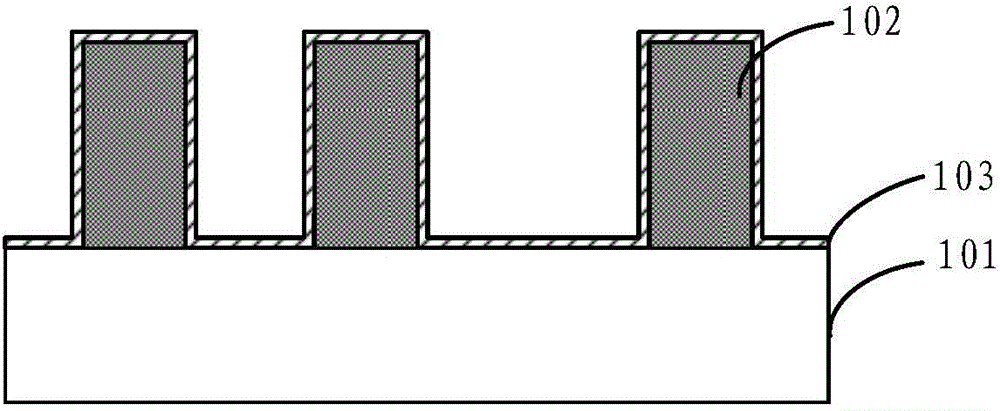
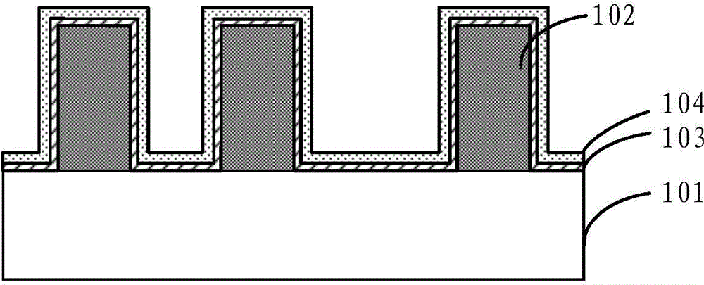
[0028] Below, refer to Figure 1a-Figure 1g and figure 2 The detailed steps of the manufacturing method of the semiconductor device proposed by the present invention will be described. Figures 1a-1g A schematic cross-sectional view of a semiconductor device obtained in key steps of a method for manufacturing a semiconductor device according to an embodiment of the present invention is shown.

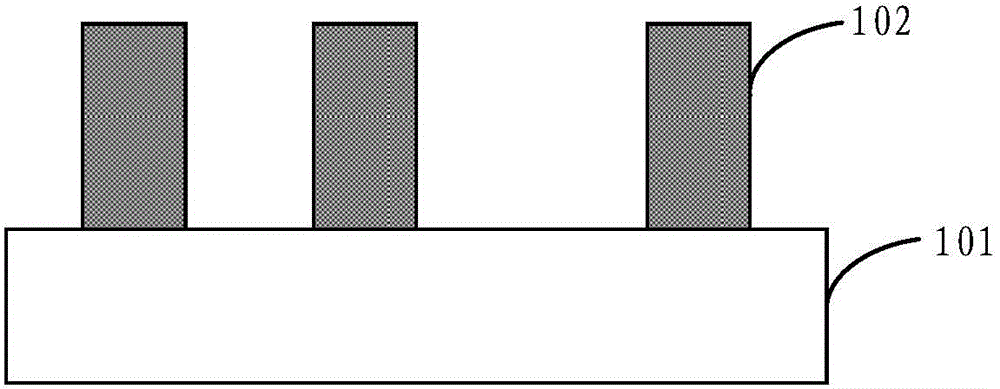
[0029] First, refer to Figure 1a , a semiconductor substrate 101 is provided, and a gate structure 102 is formed on the semiconductor substrate 101 . The constituent material of the semiconductor substrate 101 may be at least one of the materials mentioned below: silicon, silicon-on-insulator (SOI), silicon-on-insulator (SSOI), silicon-germanium-on-insulator (S-SiGeOI ), silicon germanium on insulator (SiGeOI) and germanium on insulator (GeOI), etc. Isolation trenches, buried layers, and various well structures may be formed in the semiconductor substrate 101 , which are omitted i...

Embodiment 2

[0048] The present invention also provides a semiconductor device, which is manufactured by the method described in the above-mentioned embodiments. The semiconductor device adopts an oxygen-rich liner layer, which can promote the transformation of the flowable dielectric material, avoid leaving voids in the interlayer dielectric layer, and does not need to increase the high temperature thermal annealing process to improve the gap of the dielectric layer filling. Therefore, the semiconductor device provided by the present invention has higher gap-fill capability of the dielectric layer, better quality of the dielectric layer, and lower thermal budget.

Embodiment 3

[0050] The present invention also provides an electronic device including a semiconductor device. Wherein, the semiconductor device is the semiconductor device described in the second embodiment, or the semiconductor device obtained according to the manufacturing method described in the first embodiment.

[0051] The electronic device of this embodiment can be any electronic product or equipment such as mobile phone, tablet computer, notebook computer, netbook, game console, TV set, VCD, DVD, navigator, camera, video recorder, voice recorder, MP3, MP4, PSP, etc. , can also be any intermediate product including the semiconductor device. The electronic device according to the embodiment of the present invention has better performance due to the use of the above-mentioned semiconductor device.


PUM

PropertyMeasurementUnit
thicknessaaaaaaaaaa
thicknessaaaaaaaaaa
thicknessaaaaaaaaaa

Abstract

The invention provides a semiconductor device and a manufacturing method therefore, and an electronic apparatus. The manufacturing method comprises the steps of providing a semiconductor substrate, wherein a grid electrode structure is formed in the semiconductor substrate; forming an oxygen-rich laying layer on the top and side wall of the grid electrode structure and the semiconductor substrate; performing operations of disposition and curing treatment on a flowable dielectric material circularly on the oxygen-rich laying layer to form an inter-layer dielectric layer; and performing annealing treatment. According to the manufacturing method for the semiconductor device, due to the adoption of the oxygen-rich laying layer, the conversion of the flowable dielectric material can be promoted, and voids in the inter-layer dielectric layer are avoided; a high-temperature thermal annealing treatment step is not required to improve the gap filling of the dielectric layer; and therefore, the manufacturing method can improve the gap filling capability of the dielectric layer, and can improve the quality of the dielectric layer without increasing thermal budget.

Description

technical field [0001] The present invention relates to the technical field of semiconductors, in particular to a semiconductor device, a manufacturing method thereof, and an electronic device. Background technique [0002] With the development of semiconductor integrated circuits, the feature size of semiconductor devices is getting smaller and smaller. The reduction in feature size results in an increase in the aspect ratio between the depth and width of gaps and trenches in semiconductor devices. Excessively high aspect ratios can cause problems during gap and trench fill, such as the tendency of the deposited material to overhang at the trench corners or create voids at the trench center. This can cause device performance and electrical reliability issues. The flowable chemical vapor deposition (FCVD) process is widely used in the process technology of the node below 20nm due to its excellent gap filling ability. To achieve good film quality, high temperature annealin...

Claims


Application Information

Patent Timeline
Patent Type & Authority Applications(China)
IPC IPC(8): H01L27/04H01L21/762H01L21/3105
Inventor 曾以志赵杰邓浩严琰
Owner SEMICON MFG INT (SHANGHAI) CORP
Why Eureka
Try Eureka