SRAM and logic transistors with variable height multi-gate transistor architecture

a logic transistor and multi-gate technology, applied in the field of multi-gate static random access memory (sram) transistors and multi-gate logic transistors having variable channels, can solve the problems of limiting circuit design flexibility and incurring layout penalties

Inactive Publication Date: 2008-07-03
INTEL CORP
View PDF99 Cites 288 Cited by
  • Summary
  • Abstract
  • Description
  • Claims
  • Application Information

AI Technical Summary

Problems solved by technology

Device 175 limits circuit design flexibility because the current carrying width must be incremented discretely, not continuously.
Also, because of lithographic pitch limitations, non-planar transistors like device 175 shown in FIG. 1B may incur a layout penalty relative to traditional single-gate transistors which can have their planar gate width scaled continuously.

Method used


Image

  • SRAM and logic transistors with variable height multi-gate transistor architecture
  • SRAM and logic transistors with variable height multi-gate transistor architecture
  • SRAM and logic transistors with variable height multi-gate transistor architecture

Examples


Embodiment Construction

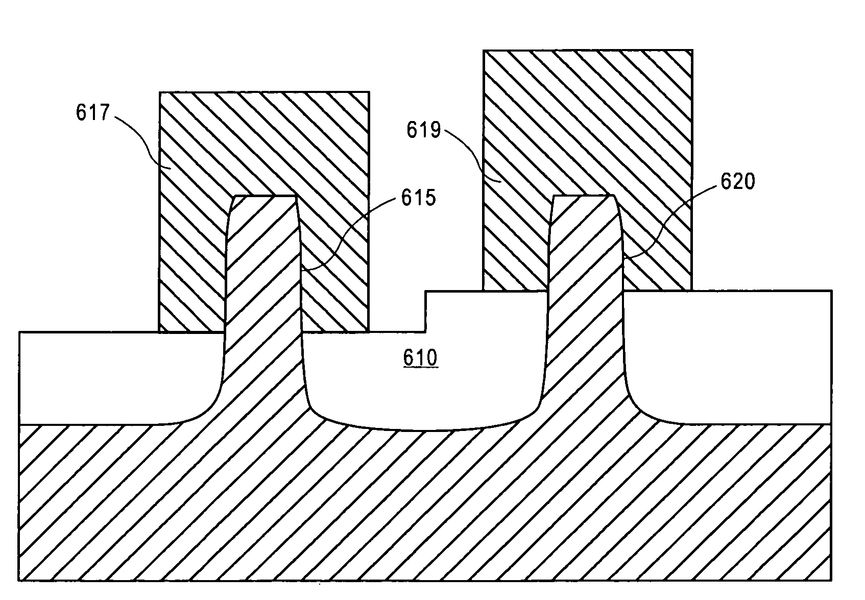
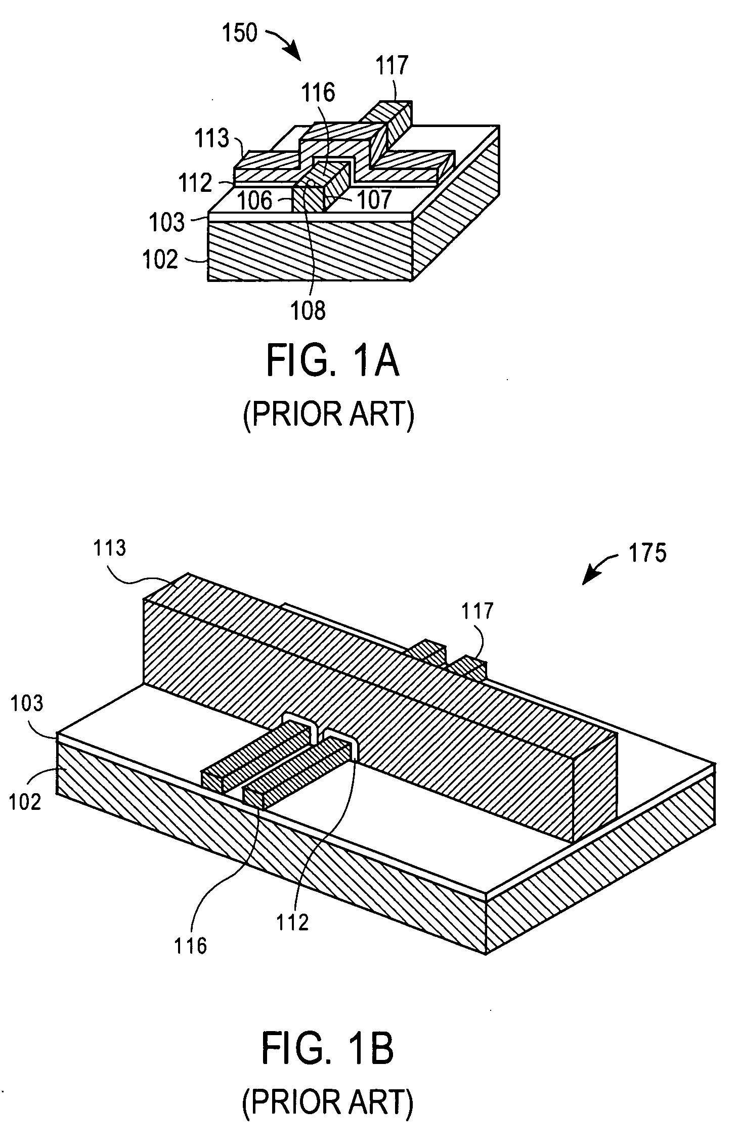
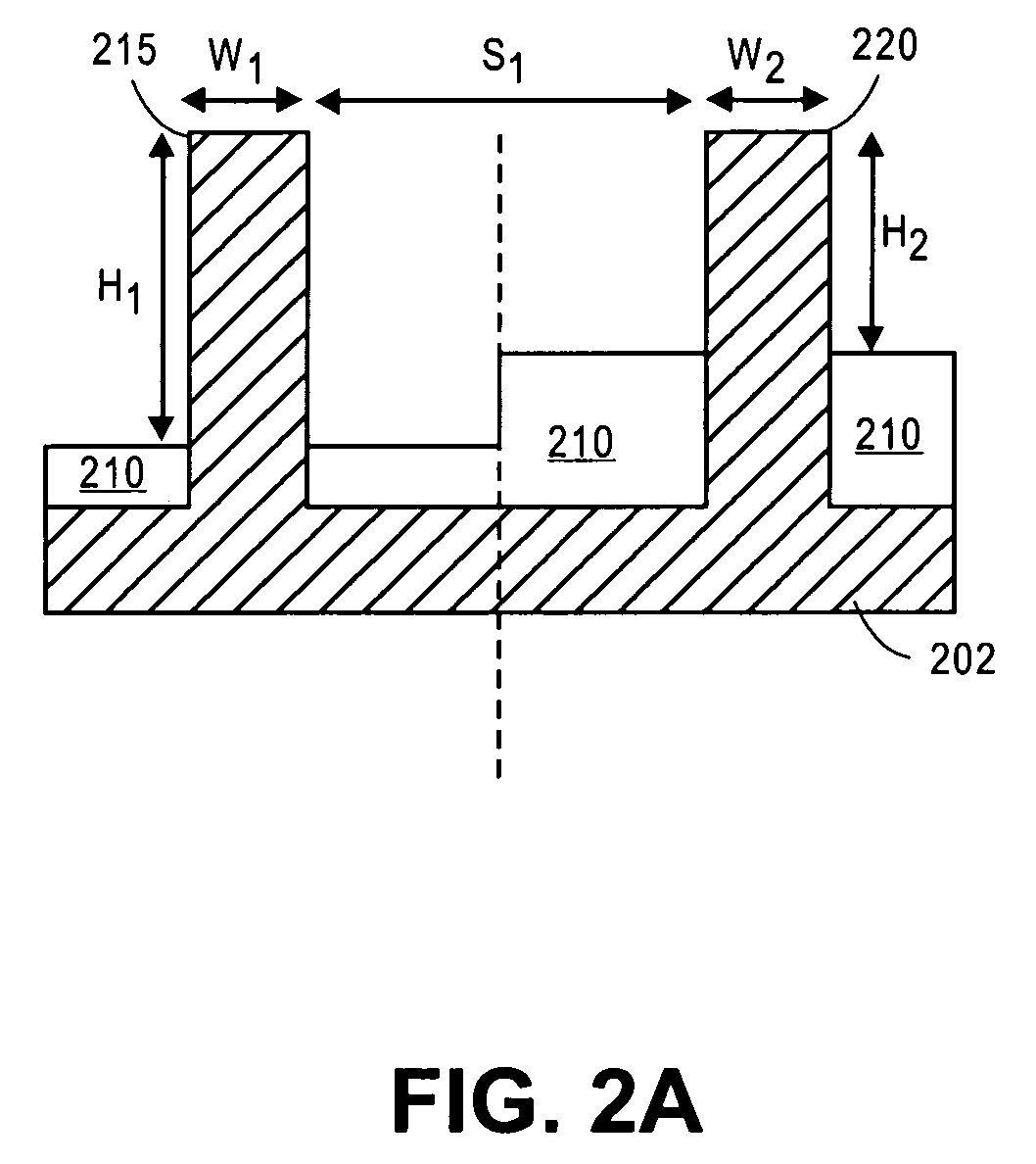
[0013]In various embodiments, multi-gate transistor architectures for SRAM and logic transistors on a single substrate are described with reference to figures. However, certain embodiments may be practiced without one or more of these specific details, or in combination with other known methods and materials. In the following description, numerous specific details are set forth, such as specific materials, dimensions and processes, etc., in order to provide a thorough understanding of the present invention. In other instances, well-known semiconductor processes and manufacturing techniques have not been described in particular detail in order to not unnecessarily obscure the present invention. Reference throughout this specification to “an embodiment” means that a particular feature, structure, material, or characteristic described in connection with the embodiment is included in at least one embodiment of the invention. Thus, the appearances of the phrase “in an embodiment” in vari...


PUM


Abstract

Multi-gate transistors having different channel widths formed on non-planar semiconductor bodies have different sidewall heights and method of manufacturing the same. In an embodiment, a multi-gate SRAM transistor is formed on a non-planar semiconductor body having a greater sidewall height than a non-planar semiconductor body utilized for a multi-gate logic transistor to improve performance of SRAM and logic transistors formed on the same substrate. In another embodiment, to reduce cell area, a first SRAM transistor is formed on a non-planar semiconductor body having a greater sidewall height than a non-planar semiconductor body utilized for a second multi-gate SRAM transistor.

Description

BACKGROUND OF THE INVENTION[0001]1. Field of the Invention[0002]The present invention relates to the field of semiconductor integrated circuit manufacturing, and more particularly to multi-gate static random access memory (SRAM) transistors and multi-gate logic transistors having variable channel widths.[0003]2. Discussion of Related Art[0004]Multi-gate transistors have been under development to address the short channel effect (SCE) afflicting planar nano-scale transistors. A multi-gate transistor is a transistor where the gate electrode couples to the channel through more than one surface plane of the semiconductor, typically through sidewall portions formed by the non-planarity. Transistor 150, as shown in FIG. 1A, is such a non-planar device. A semiconductor body, having opposite sidewalls 106 and 107, and a top surface 108, is formed over a substrate comprised of isolation 103 on a handling substrate 102. The top surface 108 and the opposite sidewalls 106 and 107 are apportione...

Claims


Application Information

Patent Timeline
Patent Type & Authority Applications(United States)
IPC IPC(8): H01L21/336H01L29/768
CPCH01L27/105H01L27/11H01L29/7851H01L27/1116H01L29/66795H01L27/1104H10B10/18H10B10/00H10B10/12
Inventor DATTA, SUMANDOYLE, BRIAN S.KAVALIEROS, JACK T.WANG, YIH
Owner INTEL CORP
Why Eureka
Try Eureka