
Eureka
For R&D, Eureka makes reading and utilizing patents & technical documents easy.
Eureka AIR
Designed for self-driven R&D workflows. Generate viable solutions, solve complex R&D challenges, empower your innovation with AI.

Eureka Materials
Designed for material experts only. Revolutionize your material R&D, from search, analyze, to developing new materials.

TechResearch
Generate reliable direction feasibility study reports for your R&D in just a few steps.

TechSeek
Discover and master advanced knowledge NOW. Basics, ideas, possibilities, all at once.

TechMind
As an expert in R&D Theories, TechMind can generates customized viable solutions instantly.

TechRisk
Analyze your overall solution with one click, know your potential R&D risks in advance.

TechMonitor
Get weekly tech updates, stay abreast of the latest tech innovations and key insights.
Inkjet printed wirebonds, encapsulant and shielding
- Summary
- Abstract
- Description
- Claims
- Application Information
AI Technical Summary
Problems solved by technology
Method used
Image

Examples
Embodiment Construction
[0001]1. Field of the Invention
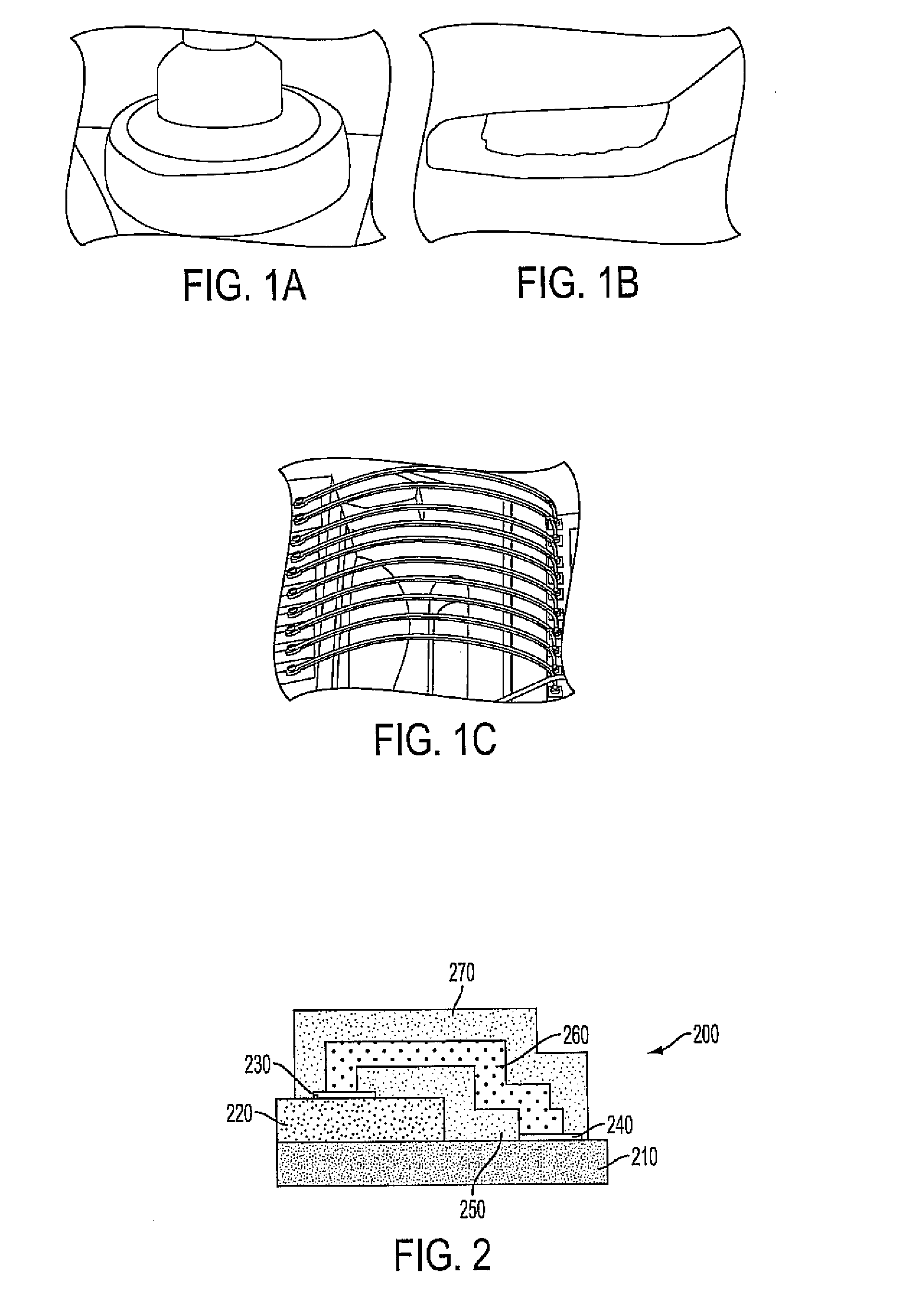
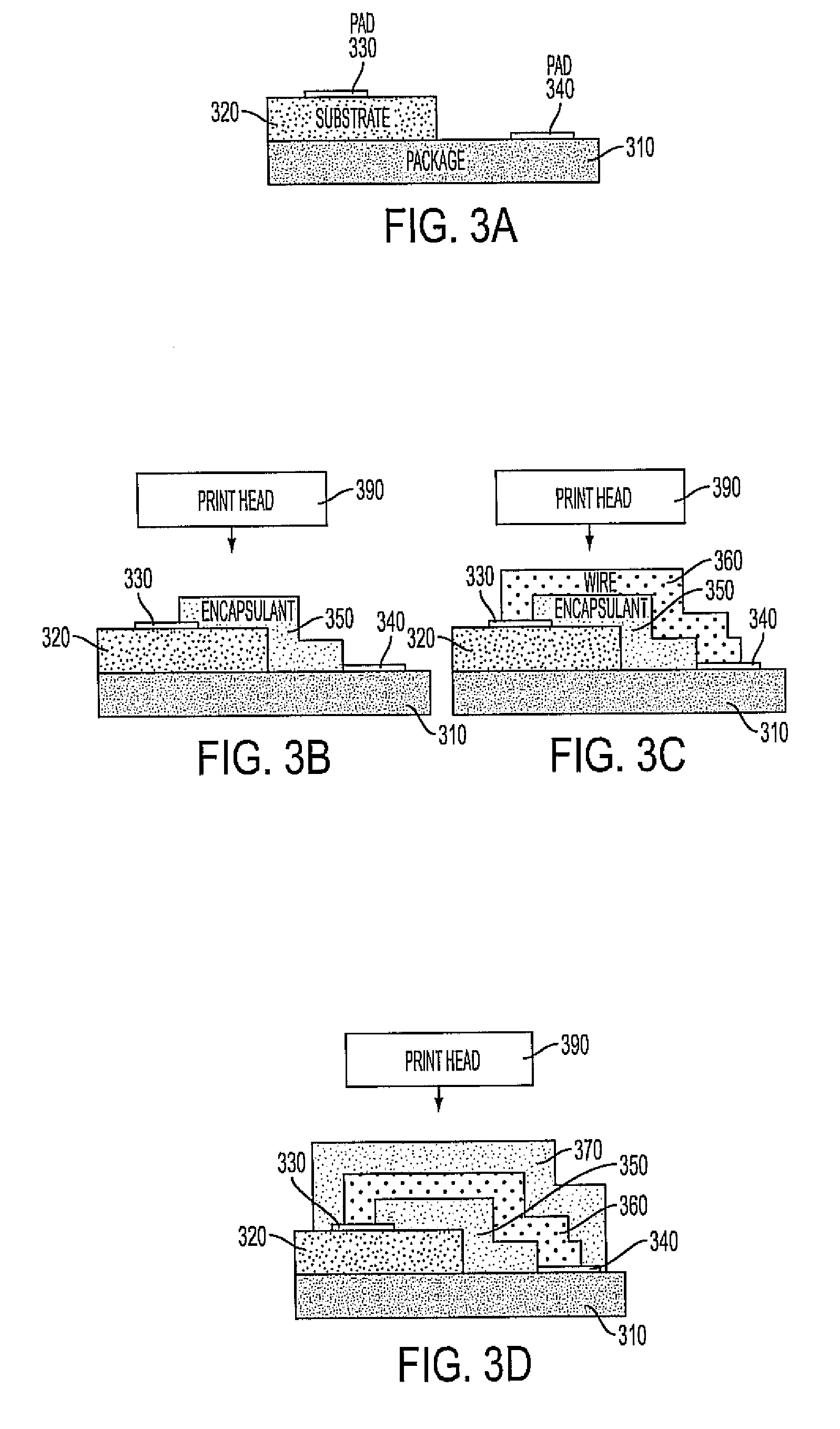
[0002]The present invention generally relates to wirebonding techniques, and more particularly, selective printing of wirebonds and spacers utilizing a materials printer.
[0003]2. Background of the Invention
[0004]Heretofore, in the fabrication of semiconductor devices, wirebonding is used to connect bond pads on a chip to bond pads on a package. More specifically, a wirebonding tool touches a pad on the chip, welding a wire to the pad, and then moving to a pad on the package while feeding a length of wire in the process. The wire is then welded at the other end thereof to the pad on the package. A path that the tool takes between the pads determines the shape and loop height of the wire, which can be important in many applications. For example, when multiple rows of pads are used to increase a density of connections, the loop heights must be controlled well enough to avoid shorting between the wires. This can be particularly important in applications su...
PUM
 Abstract
Description
Claims
Application Information
 - R&D Engineer
- R&D Manager
- IP Professional
- Industry Leading Data Capabilities
- Powerful AI technology
- Patent DNA Extraction
Browse by: Latest US Patents, China's latest patents, Technical Efficacy Thesaurus, Application Domain, Technology Topic, Popular Technical Reports.
© 2024 PatSnap. All rights reserved.Legal|Privacy policy|Modern Slavery Act Transparency Statement|Sitemap|About US| Contact US: help@patsnap.com