Light emitting display device and method for fabricating the same
- Summary
- Abstract
- Description
- Claims
- Application Information
AI Technical Summary
Benefits of technology
Problems solved by technology
Method used
Image
Examples
Embodiment Construction
[0029]Hereinafter, exemplary embodiments will be described with reference to the accompanying drawings. Here, when a first element is coupled to a second element, the first element may be directly coupled to the second element and also indirectly coupled to the second element through one or more other elements. Further, irrelevant elements are omitted for clarity. Also, like reference numerals refer to like elements throughout.
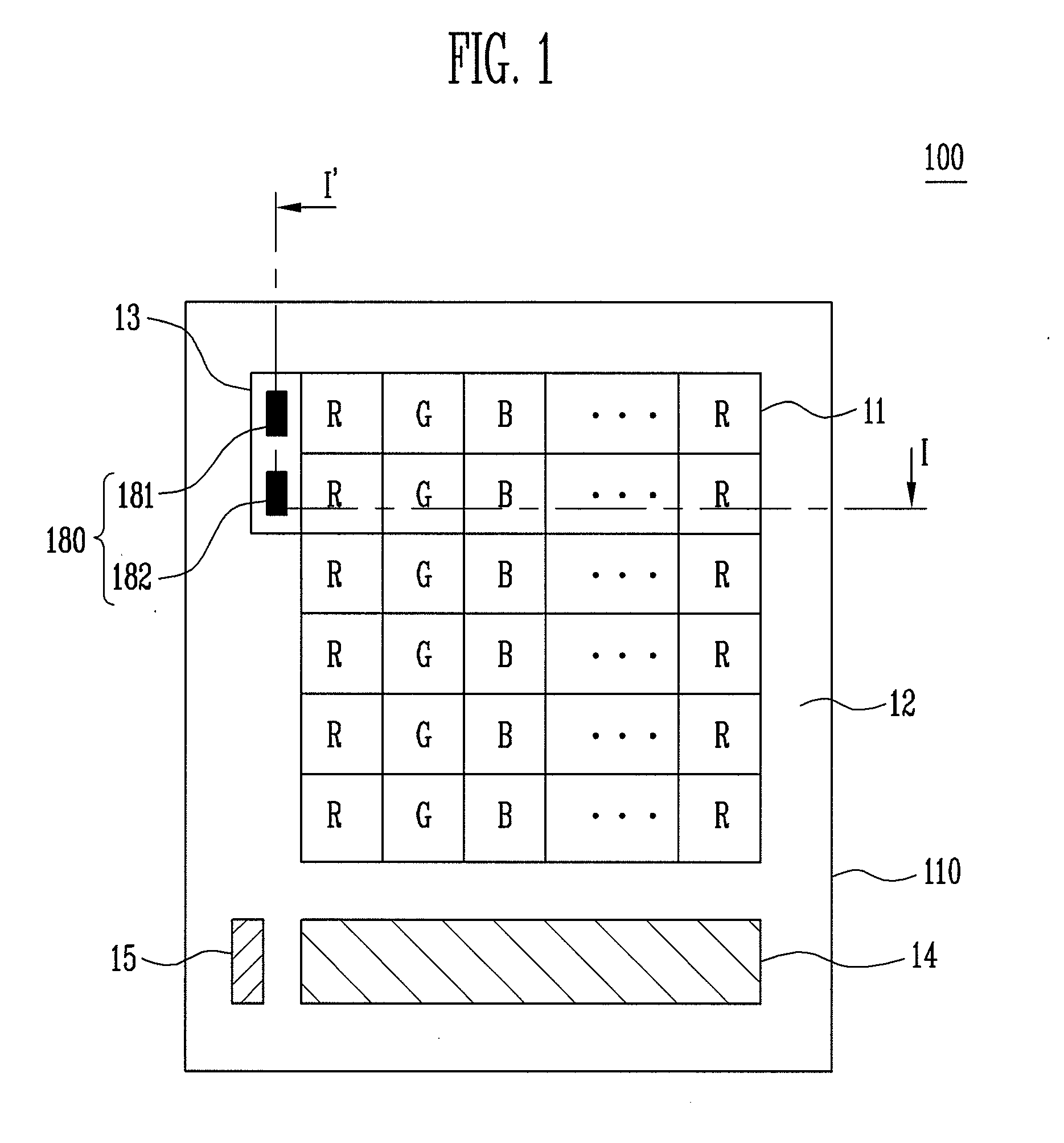
[0030]FIG. 1 is a plan view showing an organic light emitting display 100 according to a first embodiment. With reference to FIG. 1, the organic light emitting display 100 includes a substrate 110, a thin film transistor, and an organic light emitting diode.
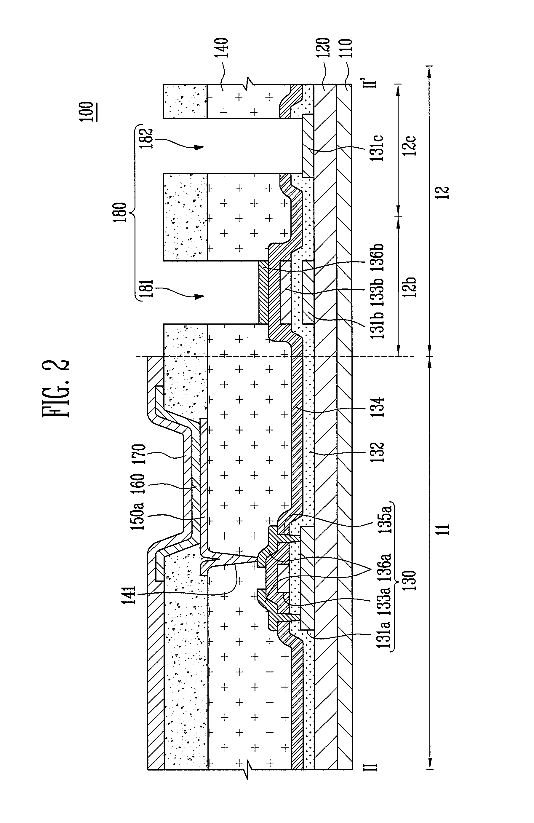
[0031]The thin film transistor is formed on a first region of the substrate 110, and includes a semiconductor layer, a gate electrode, and source / drain electrodes. The organic light emitting diode is electrically coupled to the thin film transistor, and includes a first electrode, an emission layer, and a s...
PUM
 Abstract
Description
Claims
Application Information


