
Seal Ring Structure with Improved Cracking Protection

Active Publication Date: 2008-11-20
TAIWAN SEMICON MFG CO LTD
View PDF95 Cites 45 Cited by
  • Summary
  • Abstract
  • Description
  • Claims
  • Application Information

AI Technical Summary

Benefits of technology

[0013]Advantageously, by using the embodiments of the present invention, the crack-propagation occurring due to die sawing is reduced.

Problems solved by technology

If this seal ring is damaged, there will be no structure for preventing cracks from propagating into the respective semiconductor chip.
Second, the continuous via bars often have widths substantially less than the thickness of the respective overlying metal lines, and hence do not have enough strength to stop crack propagation during die sawing.

Method used


Image

  • Seal Ring Structure with Improved Cracking Protection
  • Seal Ring Structure with Improved Cracking Protection
  • Seal Ring Structure with Improved Cracking Protection

Examples


first embodiment

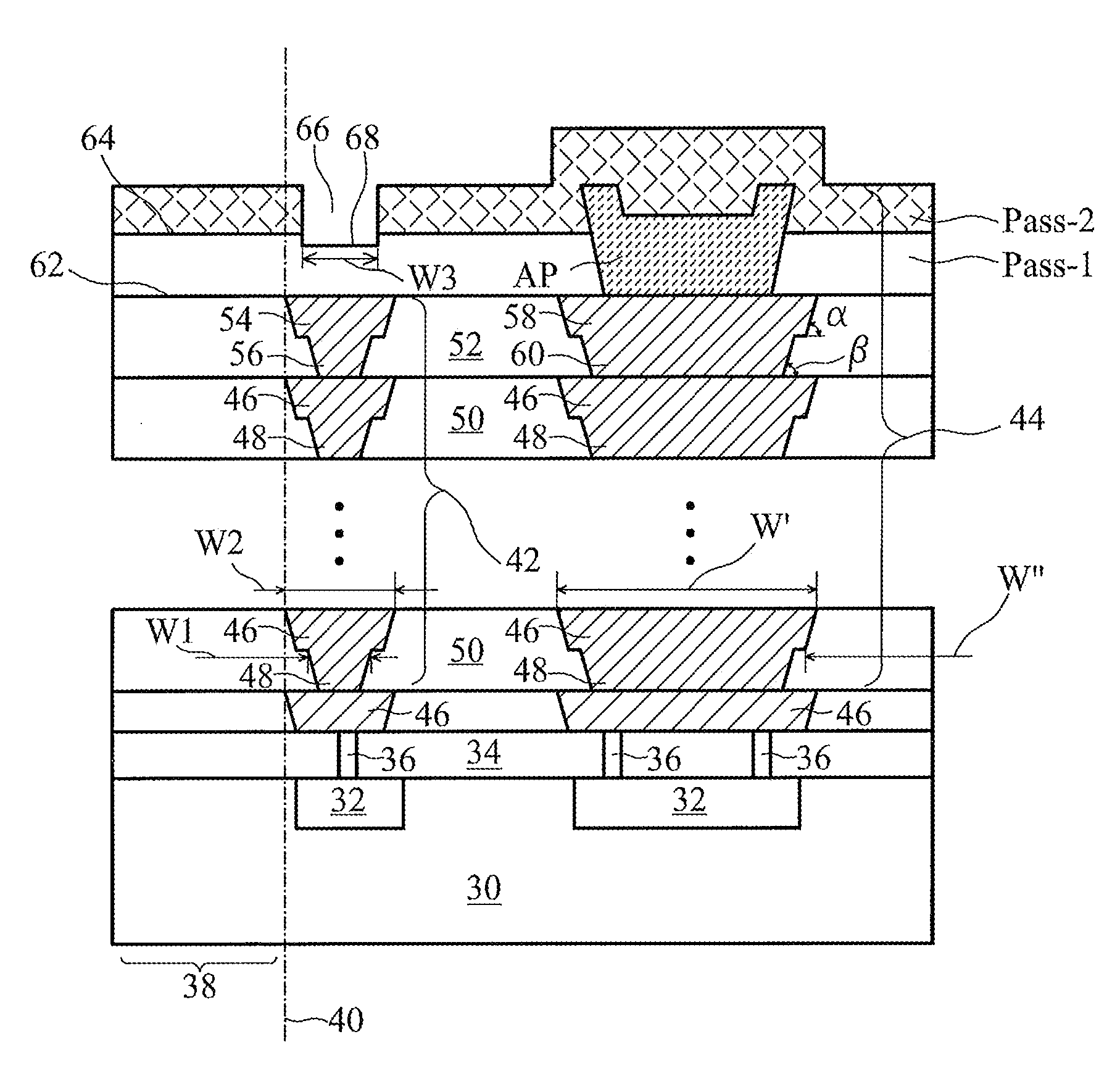
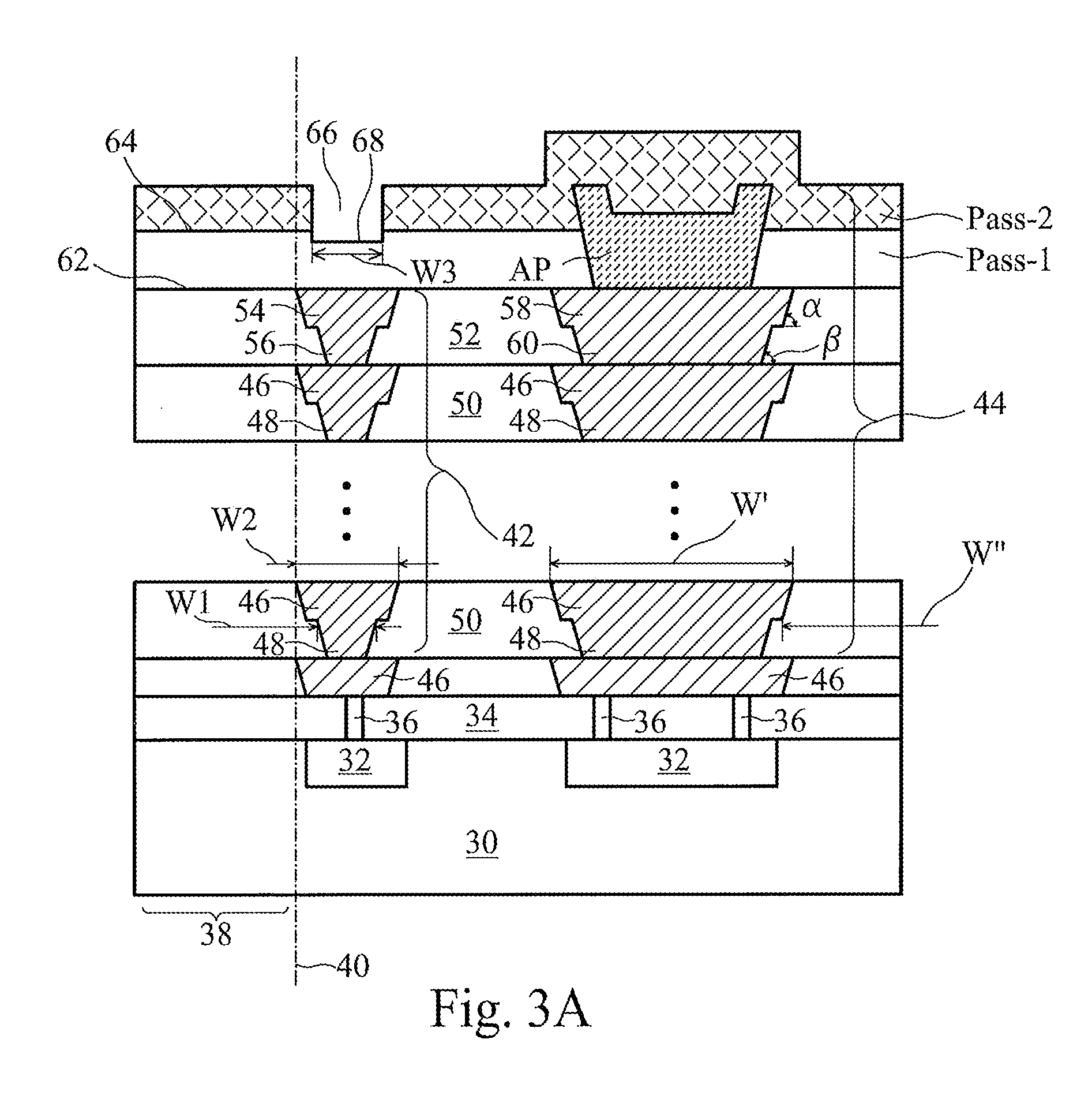
[0022]FIG. 3A illustrates the present invention. A portion of a semiconductor wafer includes semiconductor substrate 30, which is preferably formed of silicon or other group III, group IV, and / or group V elements. Preferably, semiconductor substrate 30 is lightly doped with a p-type impurity. Heavily doped p-type (p+) regions 32 are formed at the top surface of semiconductor substrate 30. Inter-layer dielectric (ILD) 34 is formed over substrate 30. ILD 34 may be formed of phosphoboronsilicate glass (PBSG) or other commonly used materials.

[0023]In an embodiment, contacts 36 are formed in ILD 34, and are electrically connected to p+ regions 32. Contacts 36 are connected to an electrical ground (not shown). A scribe line boundary 40 is illustrated, wherein scribe line 38 is to the left of scribe line boundary 40, and a semiconductor chip is to the right of scribe line boundary 40.

[0024]Two seal rings 42 and 44 are formed. In the preferred embodiment, the first seal ring 42 (alternative...

second embodiment

[0033]FIG. 4A illustrates the present invention, wherein seal ring 42 is formed away from scribe line 38. Trench 66 includes at least a portion horizontally between seal ring 42 and scribe line 38. Further, the entire trench 66 may be between seal ring 42 and scribe line 38. In this case, the bottom 68 of trench 66 may extend below the interface 62, wherein the corresponding position of bottom 68 is illustrated using a dashed line. Alternatively, bottom 68 may be substantially leveled to interface 64 or between interfaces 62 and 64. If, however, trench 66 includes a portion directly over seal ring 42, the bottom 68 is preferably higher than interface 62, so that at least one thin passivation layer Pass-1 remains over metal line 54.

[0034]Trench 66 may be located anywhere between scribe line 38 and main seal ring 44. FIG. 4B illustrates an alternative embodiment, wherein trench 66 is between seal rings 42 and 44. In this embodiment, bottom 68 of trench 66 may also be below interface 6...

third embodiment

[0035]FIG. 5 illustrates the present invention, wherein no sacrificial seal ring is formed. Seal ring 44 is spaced apart from scribe line 38. The distance D is at least great enough to accommodate trench 66. In an exemplary embodiment, distance D is greater than about 2 μm. Trench 66 is formed substantially adjoining, but outside of scribe line 38, and it is preferable that in the die sawing, the kerf will not cut through trench 66. Again, the bottom 68 of trench 66 is preferably at least level to interface 64, and more preferably between interfaces 62 and 64, and even more preferably lower than interface 62. Bottom 68 may even extend lower than metal line 58, but higher than the top low-k dielectric layer 50. The dashed lines illustrate several possible positions of bottoms 68. Advantageously, cracks propagated in USG 52 or above will be stopped by trench 66, and seal ring 44 provides an additional protection.


PUM


Abstract

An integrated circuit structure includes a semiconductor chip comprising a plurality of dielectric layers, wherein the plurality of dielectric layers includes a top dielectric layer; and a first seal ring adjacent edges of the semiconductor chip. The integrated circuit structure further includes a first passivation layer over a top dielectric layer; and a trench extending from a top surface of the first passivation layer into the first passivation layer, wherein the trench substantially forms a ring. Each side of the ring is adjacent to a respective edge of the semiconductor chip. At least one of the plurality of vias has a width greater than about 70 percent of a width of a respective overlying metal line in the plurality of metal lines.

Description

[0001]This application claims the benefit of the following provisionally filed U.S. patent application: Application Ser. No. 60 / 930,107, filed May 14, 2007, entitled “Seal Ring Structure for Semiconductor,” which patent application is incorporated herein by reference.TECHNICAL FIELD[0002]This invention relates to integrated circuits, and more particularly to structures and formation methods of seal rings.BACKGROUND[0003]Seal ring formation is an important part in the back-end of semiconductor processes. Seal rings are stress protection structures around integrated circuits, protecting the internal circuit inside semiconductor chips from damage caused by the sawing of the semiconductor chips from wafers.[0004]Typical seal rings are usually formed of interconnected metal lines and connecting vias. FIG. 1 is a schematic view of a part of seal ring 10, which is formed on an inner side of scribe line 12, sometimes also referred to as dicing line 12. Typically, there is a circuit region (...

Claims


Application Information

Patent Timeline
IPC IPC(8): H01L23/00
CPCH01L23/585H01L2924/0002H01L2924/00
Inventor JENG, SHIN-PUUHSU, SHIH-HSUNHOU, SHANG-YUNTSAI, HAO-YIYU, CHEN-HUA
Owner TAIWAN SEMICON MFG CO LTD
Learn More