Electromagnetic screen

a technology of electromagnetic radiation and electromagnetic radiation, applied in the direction of electrical equipment, antenna details, antennas, etc., can solve the problems of non-uniform surface impedance, shielding effect is “washed out”, and simple reduction of cross-sectional size of metallic and radio-absorbing screens does not give essential positive effect, etc., to achieve greater and more homogeneous surface impedance

Active Publication Date: 2009-01-29
SAMSUNG ELECTRONICS CO LTD
View PDF12 Cites 13 Cited by
  • Summary
  • Abstract
  • Description
  • Claims
  • Application Information

AI Technical Summary

Benefits of technology

[0011]The present invention provides a device that may have a greater and more homogeneous surface impedance for small screens that shield electromagnetic radiation in a working range of frequencies. The tangential component of an electric field on a surface of the device is non-zero and a tangential component of a magnetic field and hence and a surface current are close to zero. Thus, a screen according to an exemplary embodiment of the present invention is an artificial magnetic conductor (AMC). The electromagnetic wave radiated by an electric dipole or a monopole forms the area of a deep electromagnetic shadow behind the AMC. In particular, placing an electromagnetic screen, according to an exemplary embodiment of the present invention, between the aerial of mobile phone and a user's head may shield the user's head from electromagnetic radiation.

Problems solved by technology

The problem of designing screens for electromagnetic radiation has a long history.
Simple reduction of the cross-sectional sizes of metallic and radio-absorbing screens does not give an essential positive effect because electromagnetic waves may easily flow around such screens.
The tunable impedance surface disclosed in U.S. Pat. No. 6,483,480 may have a non-uniform surface impedance due to the limited size.
An undesirable result of the non-uniform impedance is the “washing out” of the effect of shielding, (i.e. its reduction on working frequencies of the screen).
Another problem with the tunable impedance surface disclosed in U.S. Pat. No. 6,483,480 is the complexity of the design in which a large number of shorting connections of all elements of a motionless lattice are connected with a conducting substrate.

Method used


Image

  • Electromagnetic screen
  • Electromagnetic screen
  • Electromagnetic screen

Examples


Embodiment Construction

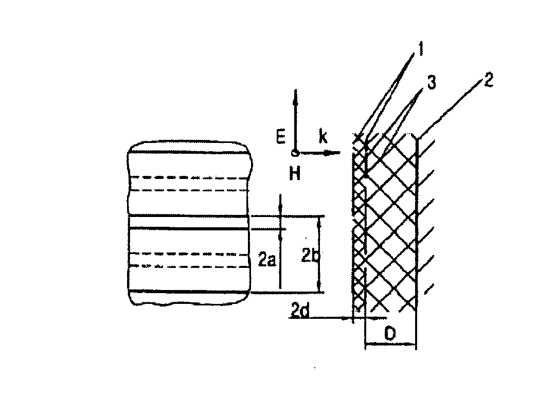
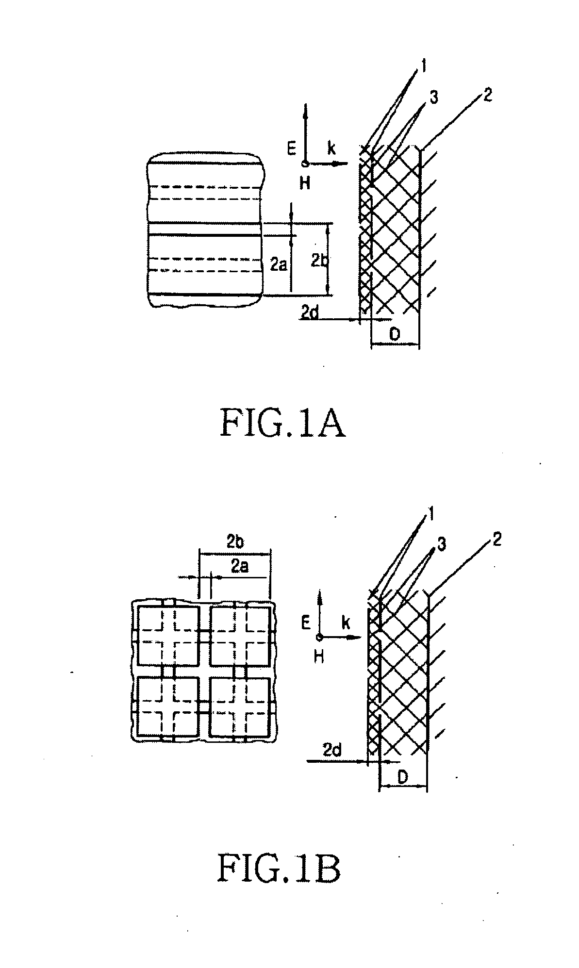
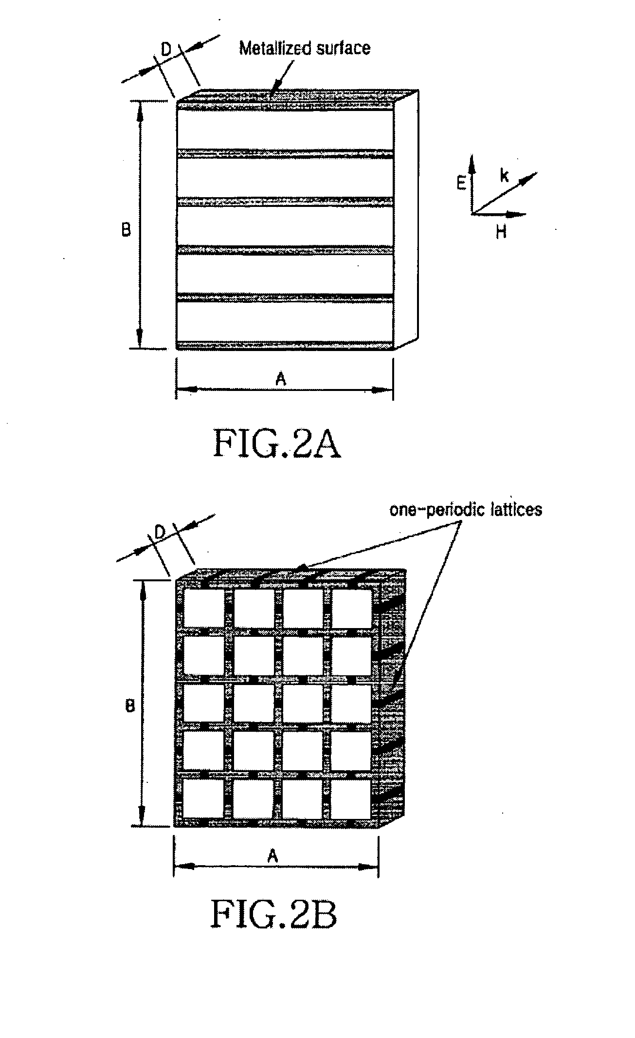
[0023]The invention is described more fully hereinafter with reference to the accompanying drawings, in which embodiments of the invention are shown. This invention may, however, be embodied in many different forms and should not be construed as limited to the embodiments set forth herein. Rather, these embodiments are provided so that this disclosure is thorough, and will fully convey the scope of the invention to those skilled in the art. In the drawings, the size and relative sizes of layers and regions may be exaggerated for clarity. Like reference numerals in the drawings denote like elements.

[0024]It will be understood that when an element or layer is referred to as being “on” or “connected to” another element or layer, it can be directly on or directly connected to the other element or layer, or intervening elements or layers may be present. In contrast, when an element is referred to as being “directly on” or “directly connected to” another element or layer, there are no int...


PUM


Abstract

The device according to an exemplary embodiment of the present invention relates to an area of wireless communication and can be used for shielding from electromagnetic radiation. The electromagnetic screen with the big surface impedance contains a flat metal reflector substrate and two lattices of capacitor type that are shifted from each other on a share of the period in parallel and located above the reflector substrate. At least one of lateral edges of the lattices has an electric connection with an edge of the reflector substrate.

Description

CROSS REFERENCE TO RELATED APPLICATION[0001]This application claims priority from and the benefit of Russian Patent Application No. 2007128677, filed on Jul. 25, 2007, which is hereby incorporated by reference for all purposes as if fully set forth herein.BACKGROUND OF THE INVENTION[0002]1. Field of the Invention[0003]The present invention relates to a device for shielding electromagnetic radiation.[0004]2. Discussion of the Background[0005]The problem of designing screens for electromagnetic radiation has a long history. Since the development of radio engineering and electronics, the question of suppression of electromagnetic communication between separate circuits and units has been dealt with. Of equal concern is the reduction of the influence of electromagnetic radiation on surrounding wildlife and humans.[0006]Conventional screens include metallic structures (metal sheets, a film, a grid etc.) and radio absorbing materials, as disclosed by O. S. Ostrovsky, et al.: “Filters and ...

Claims


Application Information

Patent Timeline
Patent Type & Authority Applications(United States)
IPC IPC(8): H05K9/00
CPCH01Q1/245H01Q15/006H01Q15/0026H01Q1/526H05K9/00
Inventor KAZANTSEV, YURY NIKOLAEVICHAPLETALIN, VLADIMIR NIKOLAEVICHKALOSHIN, VADIM ANATOLIEVICH
Owner SAMSUNG ELECTRONICS CO LTD
Why Eureka
Try Eureka