Semiconductor manufacturing apparatus and semiconductor manufacturing method using the same

Inactive Publication Date: 2009-08-13
SAMSUNG ELECTRONICS CO LTD
View PDF8 Cites 5 Cited by
  • Summary
  • Abstract
  • Description
  • Claims
  • Application Information

AI Technical Summary

Benefits of technology

[0014]However, in the semiconductor manufacturing apparatus according to a conventional art, reaction gas ions charged into a plasma state of positive pole

Problems solved by technology

However the high-temperature heat treatment process impacts the heat budget of the process, thereby decreasing an electrical characteristic of the thin film formed on a wafer in the semiconductor manufacturing process.
However, in the semiconductor manufacturing

Method used


Image

  • Semiconductor manufacturing apparatus and semiconductor manufacturing method using the same
  • Semiconductor manufacturing apparatus and semiconductor manufacturing method using the same
  • Semiconductor manufacturing apparatus and semiconductor manufacturing method using the same

Examples


Embodiment Construction

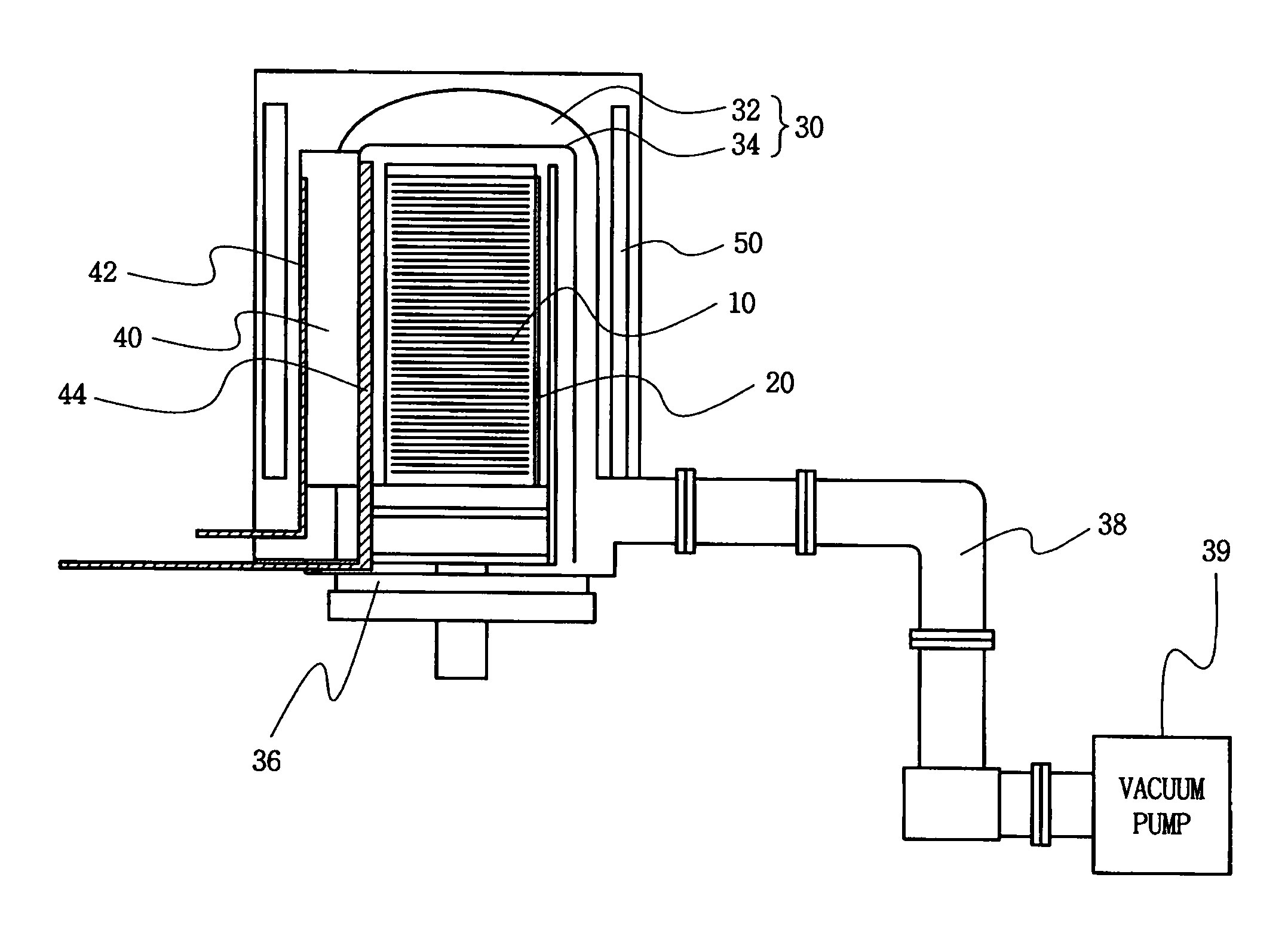
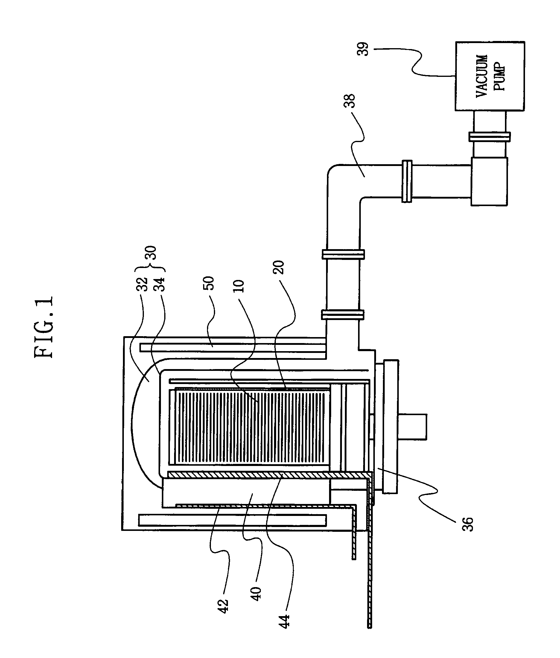
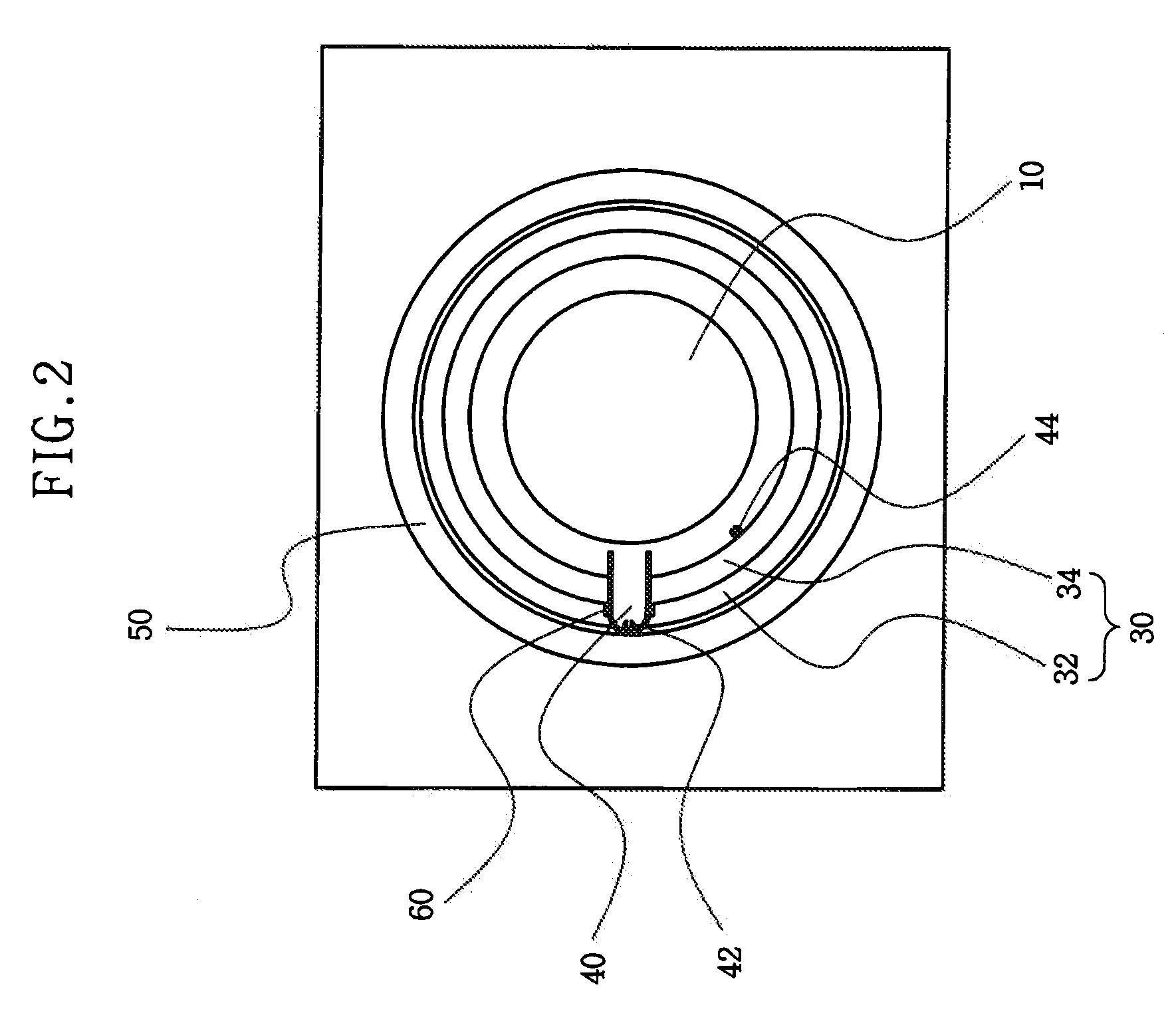
[0028]Embodiments of the present invention now will be described more fully hereinafter with reference to the accompanied drawings, in which embodiments of the invention are shown. This invention may, however, be embodied in many different forms and should not be construed as limited to the embodiments set forth herein. Rather these embodiments are provided so that this disclosure will be thorough and complete, and will fully convey the scope of the invention to those skilled in the art.

[0029]Unless otherwise defined, all terms (including technical and scientific terms) used herein have the same meaning as commonly understood by one of ordinary skill in the art to which this invention belongs. It will be further understood that terms used herein should be interpreted as having a meaning that is consistent with their meaning in the context of this specification and the relevant art and will not be interpreted in an idealized or overly formal sense unless expressly so defined herein. ...


PUM

PropertyMeasurementUnit
Polarityaaaaaaaaaa
Electric potential / voltageaaaaaaaaaa
Transparencyaaaaaaaaaa

Abstract

A semiconductor manufacturing apparatus and method are disclosed in which the apparatus comprises a reaction tube configured to hold one or more wafers, a spray pipe coupled to the reaction tube for spraying reaction gas into the reaction tube, and a plurality of electrodes used to convert the reaction gas to a plasma state. The electrodes include a cathode and an anode plasma electrode arranged for exciting reaction gas exiting the spray pipe to a plasma state prior to entry into the reaction tube. A switching device is coupled to both the cathode and anode plasma electrode and configured to switch a polarity of a high voltage applied to each of the cathode and anode to prevent a build-up of positive plasma reaction gas ions on the cathode during repeated processing steps.

Description

CROSS-REFERENCE TO RELATED APPLICATIONS[0001]This application claims priority under 35 U.S.C. §119 from Korean Patent Application 10-2008-0012485, filed on Feb. 12, 2008, the contents of which are hereby incorporated by reference in their entirety for all purposes as if fully set forth herein.BACKGROUND[0002]1. Field of the Invention[0003]The present invention relates to semiconductor manufacturing apparatuses, and more particularly, to a semiconductor manufacturing apparatus performing a deposition or diffusion process, and a semiconductor manufacturing method using the same.[0004]2. Description of the Related Art[0005]In general, semiconductor devices are manufactured through selective and repeated execution on a wafer of photo processes, etching processes, diffusion processes, ion implantation processes, etc. The purpose of the deposition and diffusion processes are to form a thin film of given thickness on the wafer in a low or high temperature atmosphere or to diffuse a conduct...

Claims


Application Information

Patent Timeline
IPC IPC(8): H01L21/223C23C16/54H01L21/30
CPCC23C16/345H01L21/2236C23C16/509H01L21/205
Inventor SEO, MOON-MIN
Owner SAMSUNG ELECTRONICS CO LTD
Why Eureka
Try Eureka