Pixel circuit, display apparatus, and pixel circuit drive control method

a technology of pixel circuit and display apparatus, applied in the direction of instruments, static indicating devices, electroluminescent light sources, etc., can solve the problems of low mobility, inconvenient control of threshold voltage, and inability to control threshold voltage, etc., to achieve high uniformity, increase power consumption, and sufficient mobility

Active Publication Date: 2009-10-01
SAMSUNG DISPLAY CO LTD
View PDF12 Cites 122 Cited by
  • Summary
  • Abstract
  • Description
  • Claims
  • Application Information

AI Technical Summary

Benefits of technology

[0036]According to the first pixel circuit and display apparatus of the present invention, inorganic oxide thin film transistors whose OFF-operation threshold voltage is a negative voltage are used as the driving transistor and switching transistor. In addition, a first capacitor element is provided between the switching transistor and a gate terminal of the driving transistor, and a second capacitor element is provided between a point located between the first capacitor element and the gate terminal of the driving transistor and a voltage source that supplies a negative voltage. This allows a voltage divided by the first and second capacitor elements to be supplied to the gate terminal of the driving transistor, so that a conventional drive circuit may be used without increasing power consumption.
[0037]According to the second pixel circuit and drive controlling method therefor of the present invention, a pixel circuit having a light emitting element and an inorganic oxide thin film transistor whose OFF-operation threshold voltage is a negative voltage is constructed, and a negative voltage is used as the gate-source voltage of the inorganic oxide thin film transistor to control the drive current of the light emitting element. This may provide advantageous features of inorganic thin film transistor, including sufficient mobility, highly uniform mobility, and low threshold voltage variation with time.

Problems solved by technology

The low-temperature polysilicon thin film transistor may provide high mobility and high stability of threshold voltage, but has a problem that the mobility is not uniform.
The amorphous silicon thin film transistor may provide uniform mobility, but has a problem that the mobility is low and threshold voltage varies with time.
The provision of the compensation circuit, however, causes the pixel circuit to become complicated, resulting in increased cost due to low yield rate and low aperture ratio.
Where thin film transistors are fabricated with inorganic oxide films in order to obtain various desired characteristics and when trying to obtain desired current characteristics, however, the threshold voltage that causes the transistors to perform OFF operation may sometimes become a negative voltage.
Further, the switching transistor is unable to fully perform OFF operation when VGS=0 v, whereby the gate voltage of the driving transistor can not be maintained.
But this method greatly increases power consumption of the display device as a whole, whereby the feature of low power consumption of EL element is spoiled.
But in order to ensure the data connection level with an external device, it is necessary to newly develop a dedicated IC, which becomes a cost increase factor of the display device.

Method used


Image

  • Pixel circuit, display apparatus, and pixel circuit drive control method
  • Pixel circuit, display apparatus, and pixel circuit drive control method
  • Pixel circuit, display apparatus, and pixel circuit drive control method

Examples


Embodiment Construction

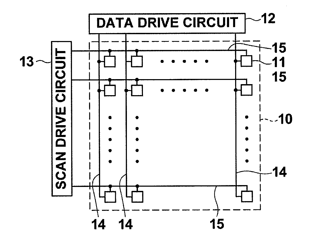
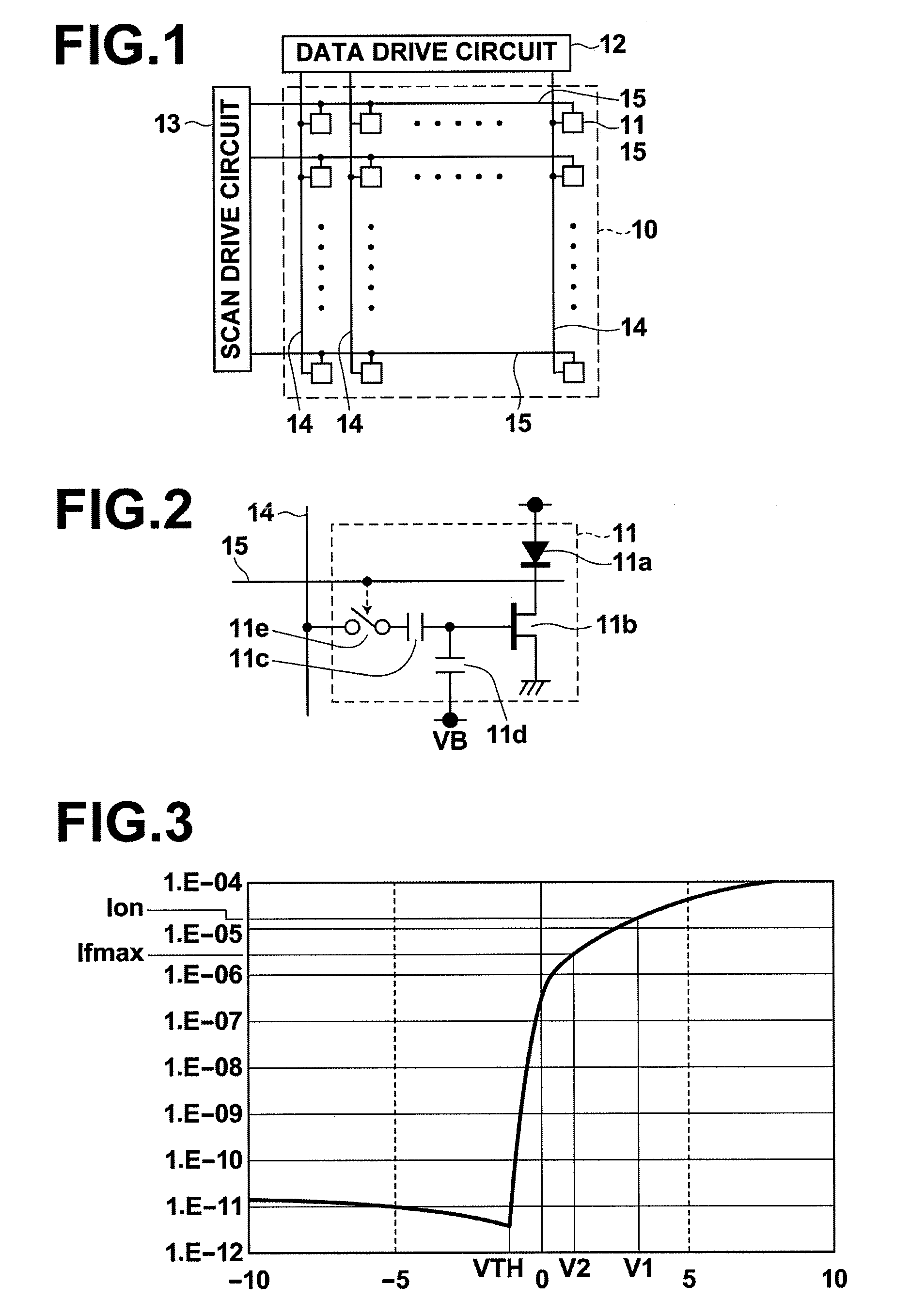
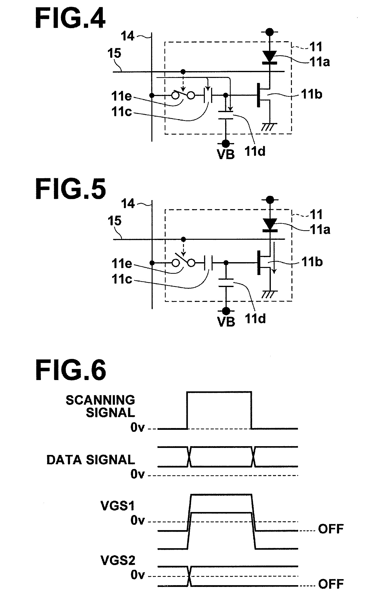
[0048]Hereinafter, an organic EL display device to which an embodiment of the pixel circuit and display apparatus of the present invention is applied will be described with reference to the accompanying drawings. FIG. 1 is a schematic configuration diagram of the organic EL display device to which an embodiment of the present invention is applied.

[0049]As shown in FIG. 1, the organic EL display device includes active matrix substrate 10 having multiple pixel circuits 11 disposed thereon two-dimensionally, each for holding charges according to a data signal outputted from a data drive circuit, to be described later, and applying a drive current to organic EL element according to the amount of charges held therein, a data drive circuit 12 that outputs a data signal to each pixel circuit 11 of the active matrix substrate 10, and a scan drive circuit 13 that outputs a scanning signal to each pixel circuit 11 of the active matrix substrate 10.

[0050]Active matrix substrate 10 further incl...


PUM


Abstract

A pixel circuit including a light emitting element, a driving transistor, connected to the light emitting element, that applies a drive current to the light emitting element, a holding circuit connected to a gate terminal of the driving transistor, and a switching transistor connected between the holding circuit and a data line through which a data signal to be held by the holding circuit flows, in which the driving transistor and the switching transistor are inorganic oxide thin film transistors whose OFF-operation threshold voltage is a negative voltage, and the holding circuit includes a first capacitor element connected between the switching transistor and the gate terminal of the driving transistor, and a second capacitor element connected between a point located between the first capacitor element and the gate terminal of the driving transistor and a voltage source that supplies a negative voltage.

Description

BACKGROUND OF THE INVENTION[0001]1. Field of the Invention[0002]The present invention generally relates to a pixel circuit and display apparatus having a light emitting element driven by active matrix method, and a pixel circuit drive control method, and more particularly to a pixel circuit using an inorganic oxide thin film transistor.[0003]2. Description of the Related Art[0004]Display devices using light emitting elements, such as organic EL element and the like, are proposed for use in various fields including televisions, cell phone displays, and the like.[0005]Generally, organic EL elements are current-driven light emitting elements, thus pixel circuits including an organic EL element proposed have a configuration like that shown in FIG. 8 as described, for example, in U.S. Pat. No. 5,684,365.[0006]The pixel circuit shown in FIG. 8 includes switching transistor 104, capacitor element 103, and driving transistor 102 as a minimum configuration. In the configuration, when switchi...

Claims


Application Information

Patent Timeline
Patent Type & Authority Applications(United States)
IPC IPC(8): G06F3/038H05B44/00
CPCG09G3/3225G09G2320/043G09G3/3266
Inventor SETO, YASUHIRO
Owner SAMSUNG DISPLAY CO LTD
Why Eureka
Try Eureka