Method of attaching an integrated circuit chip to a module

a technology of integrated circuits and modules, applied in the direction of electrical apparatus construction details, sustainable manufacturing/processing, final product manufacturing, etc., can solve the problems of chip tilting during reflow, missing solder bumps, and voids in the underfill

Inactive Publication Date: 2009-11-12
IBM CORP
View PDF54 Cites 11 Cited by
  • Summary
  • Abstract
  • Description
  • Claims
  • Application Information

AI Technical Summary

Problems solved by technology

This technology has some limitations, which include, voids in the underfill, chip tilting during reflow and missing solder bumps (particularly with low-lead and non-lead solder) to name a few.
These limitations can impact yield and reliability and require several testing and inspection steps be included in the manufacturing process adding to cost and turn-around time.

Method used


Image

  • Method of attaching an integrated circuit chip to a module
  • Method of attaching an integrated circuit chip to a module
  • Method of attaching an integrated circuit chip to a module

Examples


Embodiment Construction

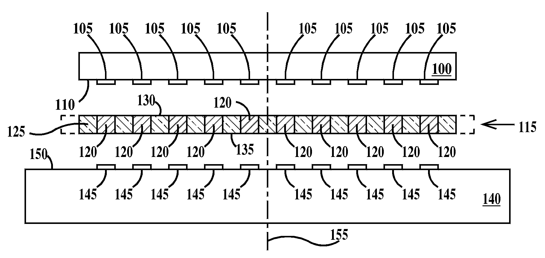
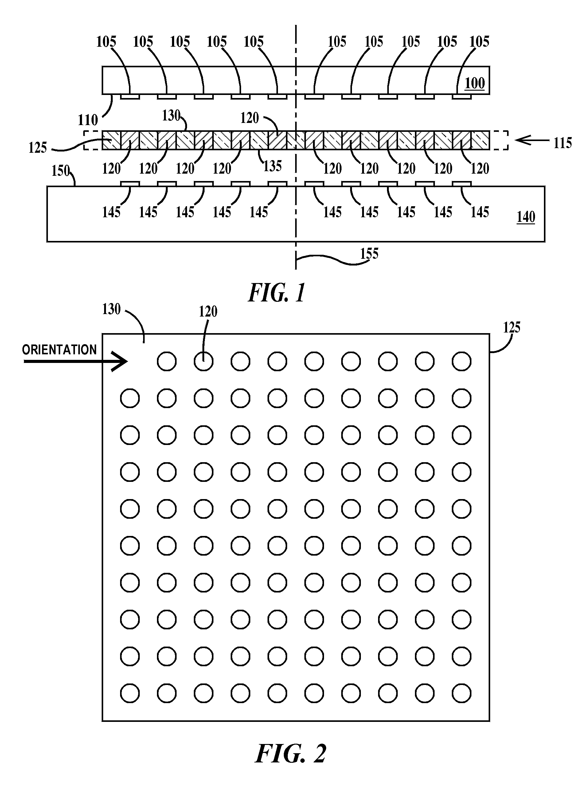
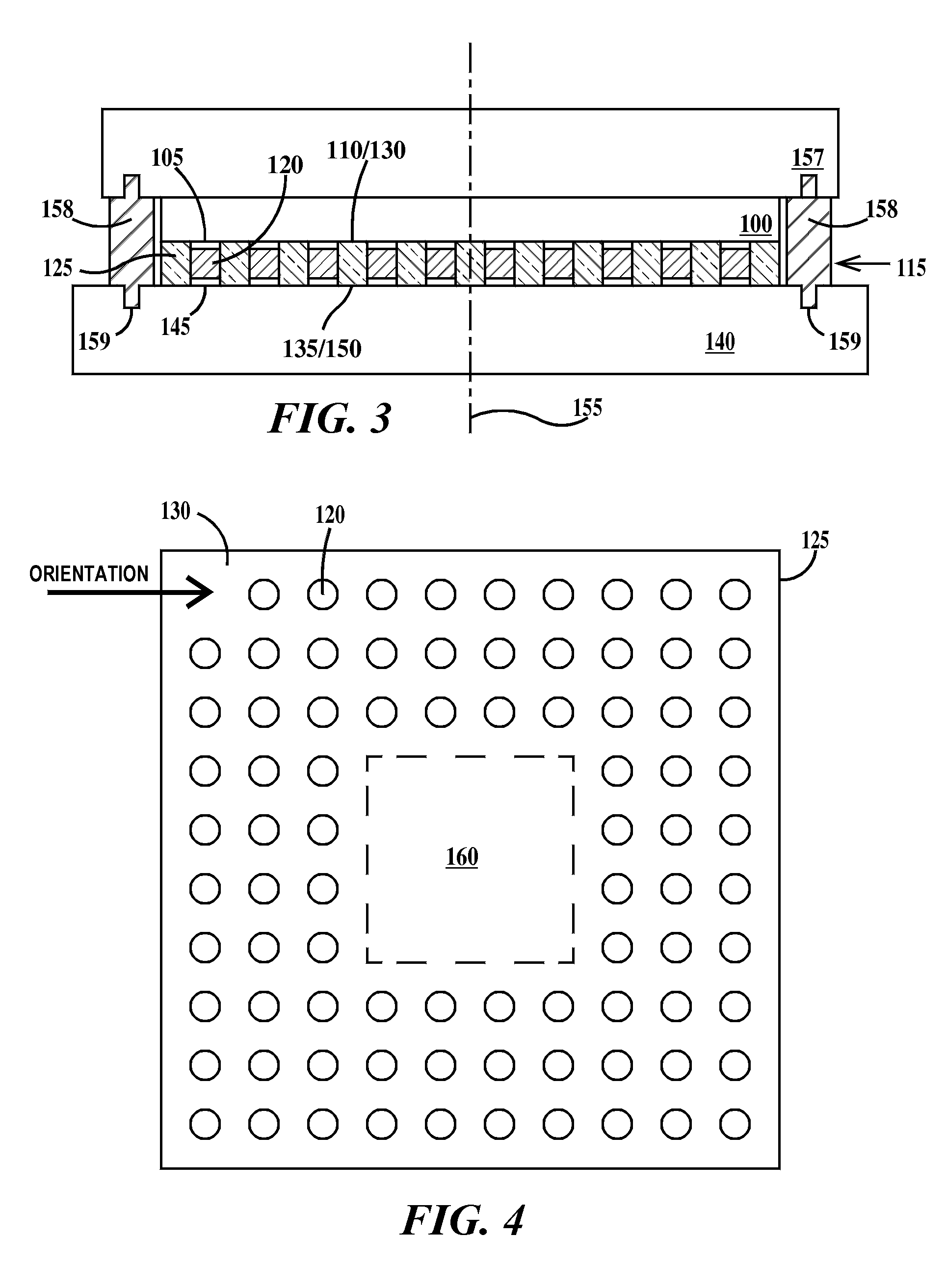
[0020]An integrated circuit module is first level packaging element intermediate between an integrated circuit chip and a second level packaging element. Examples of module types include ceramic modules (wires on or embedded in a ceramic substrate), multilayer ceramic modules (multiple levels of wires on and / or embedded in multiple layers of ceramic material) and printed circuit modules. Examples of second level packages include but are not limited to printed circuit boards and cards. Printed circuit boards / card and printed circuit modules may include one or more wiring levels embedded in and / or on one or more surfaces of an organic based dielectric material (which may include non-organic materials like fiberglass).

[0021]A lead-free interconnect is defined as metallurgical interconnect containing none to less than about 0.01% lead. A low lead interconnect is defined as a metallurgical interconnect containing less than about 5% lead. When heated, solder reacts with metallic pads to f...


PUM

PropertyMeasurementUnit
dielectricaaaaaaaaaa
perimeteraaaaaaaaaa
structureaaaaaaaaaa

Abstract

A method of attaching an integrated circuit chip to a module and a resultant structure. The method includes placing a solder bump tape between the chip and the module, the solder bump tape including an array of solder columns embedded in a dielectric sheet; aligning and contacting top surfaces of solder columns with respective chip pads of an array of chip pads of the chip and aligning and contacting bottom surfaces of the solder columns with respective module pads of an array of module pads; and reflowing the solder columns to form solder interconnections between chip pads and respective module pads.

Description

FIELD OF THE INVENTION[0001]The present invention relates to the field of integrated circuit packaging; more specifically, it relates to a method and structure for electrically and mechanically connecting integrated circuit chips to modules.BACKGROUND OF THE INVENTION[0002]A common technology for electrically attaching integrated circuit chips to modules is variously called flip-chip attachment, controlled collapse chip connection (C4) attachment and solder bump attachment. In this technology, solder columns are formed on pads on the integrated circuit chip and then the chip is placed on a module so the solder bumps are sitting on corresponding pads. The solder bumps are then heated so they melt (reflow) and physically and electrically connect the chip pads to the module pads. Then a dielectric underfill material is injected between the module and integrated circuit chip, filling the space between solder bumps. This technology has some limitations, which include, voids in the underf...

Claims


Application Information

Patent Timeline
Patent Type & Authority Applications(United States)
IPC IPC(8): H05K7/02H01L21/60
CPCH01L24/14Y10T29/49213H01L24/75H01L24/81H01L24/83H01L2224/13099H01L2224/16H01L2224/75H01L2224/81101H01L2224/81121H01L2224/81205H01L2224/81801H01L2224/838H01L2924/01029H01L2924/0103H01L2924/01047H01L2924/01049H01L2924/0105H01L2924/01051H01L2924/01082H01L2924/14H05K3/3436H05K3/3478H05K7/1061H05K2201/10424H05K2203/0415H01L2224/2919H01L2924/01033H01L2924/014H01L2924/0665H01L24/28H01L2924/00H01L24/05H01L24/06H01L24/13H01L24/29H01L2224/05568H01L2224/05573H01L2224/0613H01L2224/06134H01L2224/06135H01L2224/131H01L2224/29076H01L2224/291H01L2224/83101H01L2224/83801H01L2224/83862H01L2224/83885H01L2924/00014H01L2924/15787Y02P70/50H01L2224/05599
Inventor AYOTTE, STEPHEN PETERHILL, DAVID J.SULLIVAN, TIMOTHY M.
Owner IBM CORP
Why Eureka
Try Eureka