Plasma cleaning method and plasma CVD method

a cleaning method and plasma technology, applied in the field of plasma cleaning method and plasma cvd method, can solve the problems of insufficient studies concerning the conditions of performing the cleaning process at high throughput to achieve the cleaning effect practically sufficient, adversely affect the film formation performed in the plasma cvd apparatus, and deteriorate the film formation rate and/or film formation uniformity, etc., to achieve the effect of improving the uniformity of the plasma cvd process, high throughput and high throughpu

a cleaning method and plasma technology, applied in the field of plasma cleaning method and plasma cvd method, can solve the problems of insufficient studies concerning the conditions of performing the cleaning process at high throughput to achieve the cleaning effect practically sufficient, adversely affect the film formation performed in the plasma cvd apparatus, and deteriorate the film formation rate and/or film formation uniformity, etc., to achieve the effect of improving the uniformity of the plasma cvd process, high throughput and high throughpu

US20090308840A1Active Publication Date: 2009-12-17TOKYO ELECTRON LTD

Image

  • Plasma cleaning method and plasma CVD method
  • Plasma cleaning method and plasma CVD method
  • Plasma cleaning method and plasma CVD method

Examples


Embodiment Construction

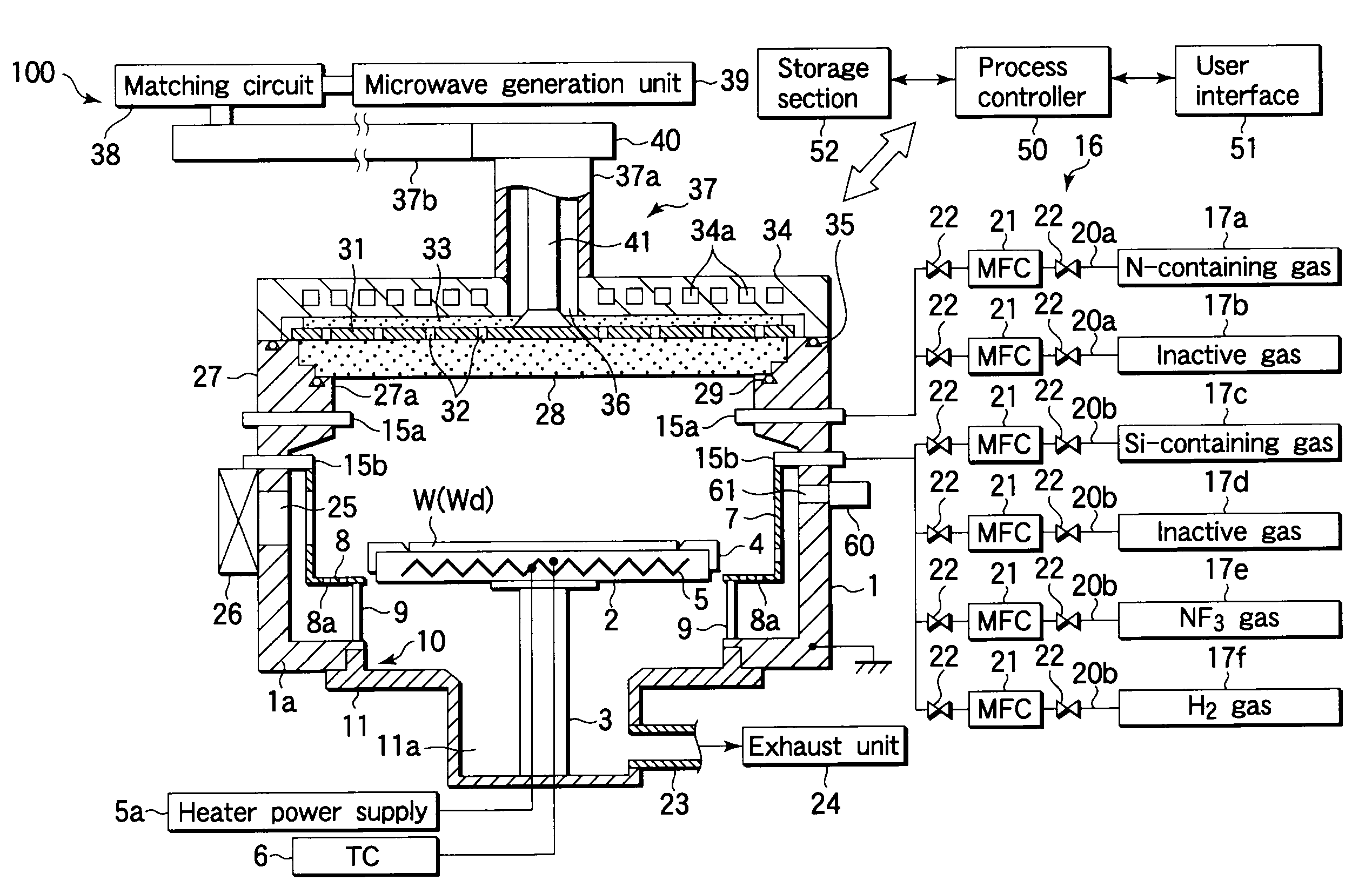
[0033]An embodiment of the present invention will now be described in detail with reference to the accompanying drawings. FIG. 1 is a sectional view schematically showing an example of a plasma processing apparatus suitable for performing a plasma cleaning method and a plasma CVD method according to the present invention. This plasma processing apparatus 100 is arranged as a processing apparatus of the RLSA (Radial Line Slot Antenna) microwave plasma type, in which microwaves are supplied from a planar antenna having a plurality of slots into a process chamber to generate plasma. In this case, microwave excitation plasma is generated with a high density and a low electron temperature, such as a plasma density of 1×10¹⁰ to 5×10¹² / cm3 and a low electron temperature of 0.7 to 2 eV, and so a process can be performed with very little damage to the film. Accordingly, apparatuses of this type are preferably utilized for processes, such as formation of a silicon nitride film by plasma CVD, ...


PUM

PropertyMeasurementUnit
temperatureaaaaaaaaaa
inner pressureaaaaaaaaaa
frequencyaaaaaaaaaa

Abstract

A plasma cleaning method is performed in a plasma CVD apparatus for depositing a silicon nitride film on a surface of a target substrate, and includes a stage (S1) of supplying a cleaning gas containing NF3 gas into a process container, thereby removing extraneous deposits formed on portions inside the process container; a stage (S2) of supplying a gas containing hydrogen gas into the process container and generating plasma thereof, thereby removing residual fluorine inside the process container; and a stage (S3) of supplying a gas containing a rare gas into the process container and generating plasma thereof, thereby removing residual hydrogen inside the process container.

Description

TECHNICAL FIELD[0001]The present invention relates to a plasma cleaning method for cleaning the interior of a process container of a plasma CVD (Chemical Vapor Deposition) apparatus that is used for depositing a silicon nitride film on the surface of a target substrate, and also relates to a plasma CVD method.BACKGROUND ART[0002]Silicon nitride films are used as insulating films, protection films, and so forth in various semiconductor device. It is known that a silicon nitride film of this kind can be formed by plasma CVD or the like using a silicon-containing compound gas, such as silane (SiH4), as a source gas and a nitrogen-containing compound gas, such as nitrogen or ammonia.[0003]In a plasma CVD apparatus for performing plasma CVD as described above, as the film formation is repeated on target substrates, silicon nitride is deposited on portions inside the chamber other than the target substrates. If extraneous deposits thus formed on portions inside the chamber exceed a certai...

Claims


Application Information

Patent Timeline
17 Dec 2009
Publication
US20090308840A1
IPC
C23F1/00; C23F1/08
CPC
C23C16/4405; H01L21/3185; H01J37/32862; H01L21/02274; H01L21/02211; H01L21/0217; H01L21/31; H01L21/3065
Inventors
KOHNO, MASAYUKI; NISHITA, TATSUO