Unlock instant, AI-driven research and patent intelligence for your innovation.

Nonvolatile semiconductor memory device and method for manufacturing same

a semiconductor memory and non-volatile technology, applied in the direction of semiconductor devices, basic electric elements, electrical appliances, etc., can solve the problems of increasing the number of lithography steps, difficult cost reduction, and difficulty in downscaling in terms of technology and cos

Inactive Publication Date: 2009-12-31
KK TOSHIBA
View PDF5 Cites 64 Cited by
  • Summary
  • Abstract
  • Description
  • Claims
  • Application Information

AI Technical Summary

Benefits of technology

The invention provides a nonvolatile semiconductor memory device with a stacked body, a through hole, and a charge storage layer. The method for manufacturing the device includes forming the stacked body, etching the electrode films and insulating film to create a recess, adding a block insulating layer and a tunnel insulating layer, and burying a semiconductor pillar inside the through hole. The technical effects include improved data retention and stability, reduced power consumption, and improved performance.

Problems solved by technology

However, such downscaling has been difficult in terms of cost and technology.
Thus, cost reduction is difficult despite three-dimensional construction.
Furthermore, because the stacked body can be simultaneously processed to fabricate a three-dimensional stacked memory, increase in the number of stacked layers does not result in increasing the number of lithography steps, and cost increase can be limited.
However, the simultaneously processed three-dimensional stacked memory thus fabricated has a problem of increased interference between memory cells as its downscaling proceeds.

Method used


Image

  • Nonvolatile semiconductor memory device and method for manufacturing same
  • Nonvolatile semiconductor memory device and method for manufacturing same
  • Nonvolatile semiconductor memory device and method for manufacturing same

Examples


Embodiment Construction

[0024]An embodiment of the invention will now be described with reference to the drawings.

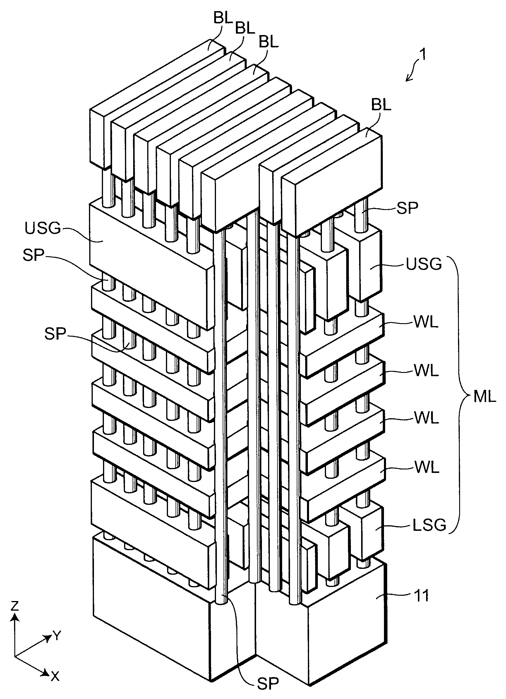
[0025]FIG. 1 is a perspective view illustrating a nonvolatile semiconductor memory device according to this embodiment.

[0026]FIG. 2 is a cross-sectional view illustrating the nonvolatile semiconductor memory device according to this embodiment.

[0027]FIG. 3 is a partially enlarged cross-sectional view illustrating region A shown in FIG. 2.

[0028]It is noted that in FIG. 1, for clarity of illustration, only the conductive portions are shown, and illustration of the insulating portions is omitted. Furthermore, FIG. 2 shows only part of one silicon pillar and its surroundings in the nonvolatile semiconductor memory device shown in FIG. 1.

[0029]As shown in FIGS. 1 and 2, the nonvolatile semiconductor memory device 1 (hereinafter also simply referred to as “device 1”) according to this embodiment is a three-dimensionally stacked flash memory. As described later, in the device 1, cell transistors are a...


PUM


Abstract

A nonvolatile semiconductor memory device includes: a stacked body with a plurality of insulating films and electrode films alternately stacked therein, through which a through hole extending in the stacking direction is formed; a semiconductor pillar buried inside the through hole; and a charge storage layer located on both sides of each of the electrode films in the stacking direction and insulated from the electrode film and the semiconductor pillar.

Description

CROSS-REFERENCE TO RELATED APPLICATIONS[0001]This application is based upon and claims the benefit of priority from the prior Japanese Patent Application No. 2008-171009, filed on Jun. 30, 2008; the entire contents of which are incorporated herein by reference.BACKGROUND OF THE INVENTION[0002]1. Field of the Invention[0003]This invention relates to a nonvolatile semiconductor memory device with a plurality of insulating films and a plurality of electrode films alternately stacked therein, and a method for manufacturing the same.[0004]2. Background Art[0005]Conventionally, nonvolatile semiconductor memory devices such as flash memories have been fabricated by two-dimensionally integrating elements on the surface of a silicon substrate. In this type of flash memory, downscaling by decreasing the dimensions of each element is required to reduce cost per bit and increase memory capacity. However, such downscaling has been difficult in terms of cost and technology.[0006]Numerous ideas fo...

Claims


Application Information

Patent Timeline
Patent Type & Authority Applications(United States)
IPC IPC(8): H01L29/792H01L21/336H01L21/20
CPCH01L27/11568H01L29/42348H01L27/11582H01L27/11578H10B43/20H10B43/30H10B43/27
Inventor KIDOH, MASARUTANAKA, HIROYASUKOMORI, YOSUKEISHIDUKI, MEGUMIKATSUMATA, RYOTAKITO, MASARUFUKUZUMI, YOSHIAKIAOCHI, HIDEAKI
Owner KK TOSHIBA