Scanner Based Optical Proximity Correction System and Method of Use

a scanner and optical proximity technology, applied in the field of optical proximity correction (opc) system and method of use, can solve the problems of inability to produce finer circuit patterns in newer generation technologies,

Active Publication Date: 2010-03-04
NIKON CORP +1
View PDF2 Cites 36 Cited by
  • Summary
  • Abstract
  • Description
  • Claims
  • Application Information

AI Technical Summary

Problems solved by technology

Semiconductor manufacturing is limited by the lithography process, which prints increasingly finer circuit patterns.
In the current generation of microelectronics it has become increasingly more difficult to produce finer circuit patterns.
For example, feature size, line width, and the separation between features and lines are becoming increasingly smaller and more difficult to produce in newer generation technologies, e.g., 45 nm technologies.
One of the fundamental reasons for these difficulties is that imaging of integrated circuit (IC) patterns has become prone to optical proximity effects (OPEs) modifying the images in a interdependent manner where any pattern interacts with imaging of its neighbors.
However, the accuracy of OPC models have not kept pace with the requirements for finer circuit patterns, leading to higher manufacturing costs, increased time to market and decreased quality in manufacturing.
Basically, the OPC models used thus far are incomplete because they do not include all the factors impacting OPEs.
However, manipulating the data to arrive at a corrected data set is a time consuming process, requiring an iterative process.
Typically, this is an intensively manual process, requiring best guesses and estimations.
This is time consuming and prone to errors and / or omissions.

Method used


Image

  • Scanner Based Optical Proximity Correction System and Method of Use
  • Scanner Based Optical Proximity Correction System and Method of Use
  • Scanner Based Optical Proximity Correction System and Method of Use

Examples


Embodiment Construction

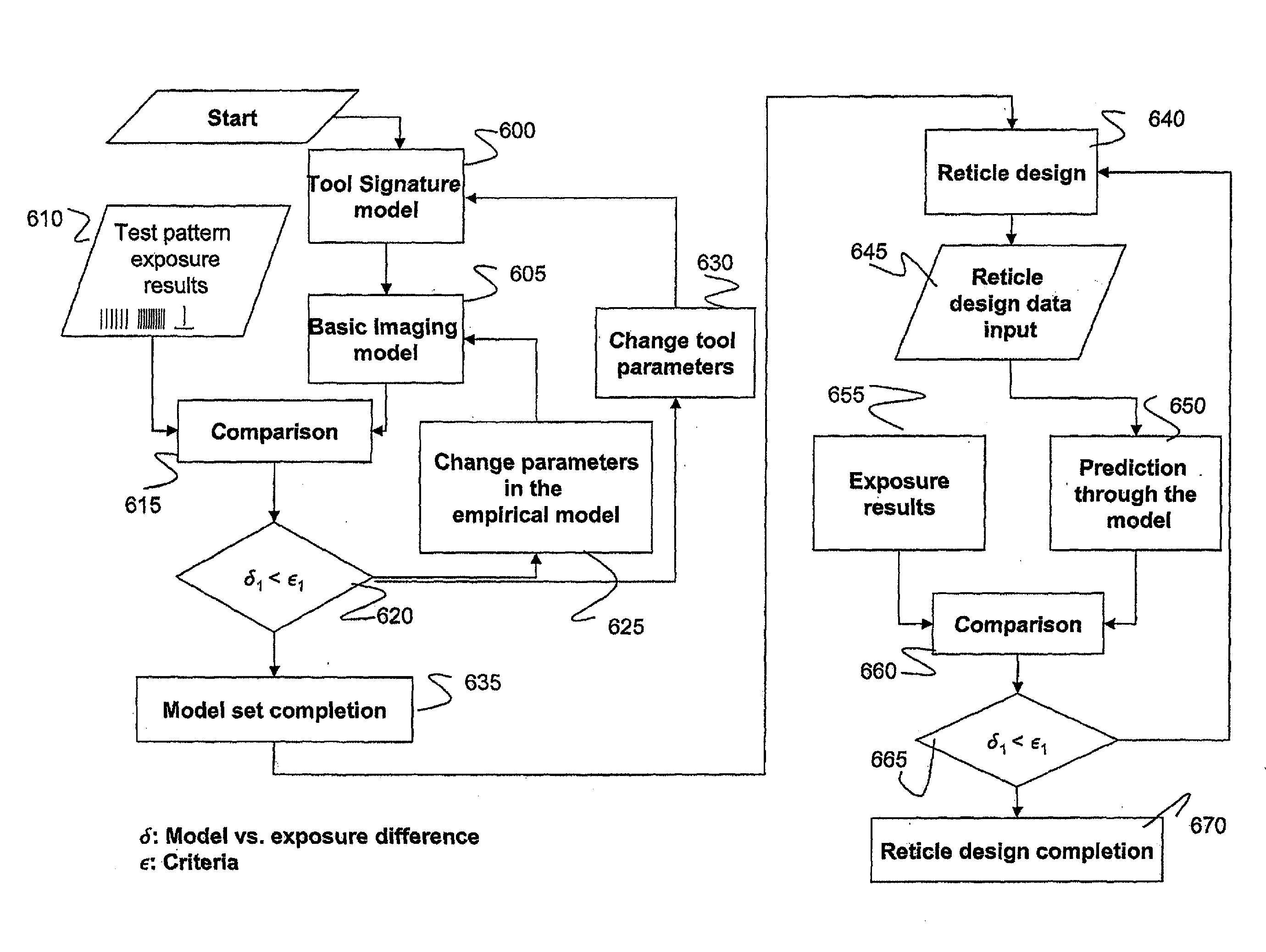
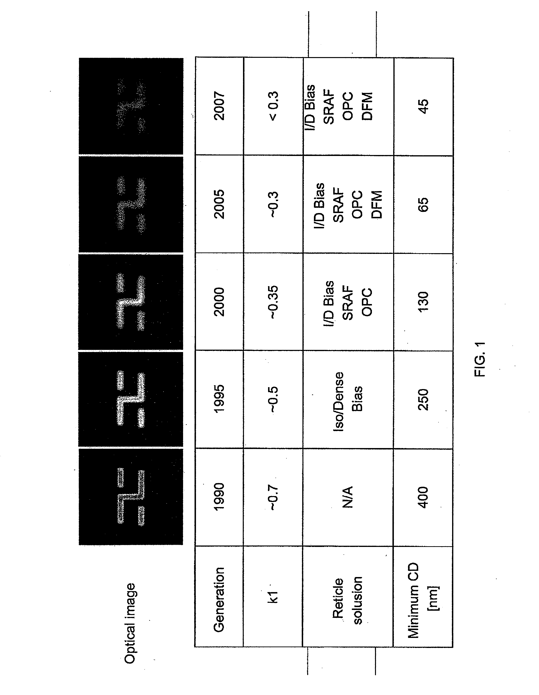
[0031]The invention generally relates to a scanner based optical proximity correction (OPC) system and method of use. In embodiments, the present invention utilizes lithography simulation and OPC models to improve critical dimension (CD) performance of integrated circuits. In preferred embodiments, the OPC models implementing the techniques described herein will improve CD performance of integrated circuits for 45 nm CD and below. The present invention can be implemented for any tool such as a scanner or a full field stepper.

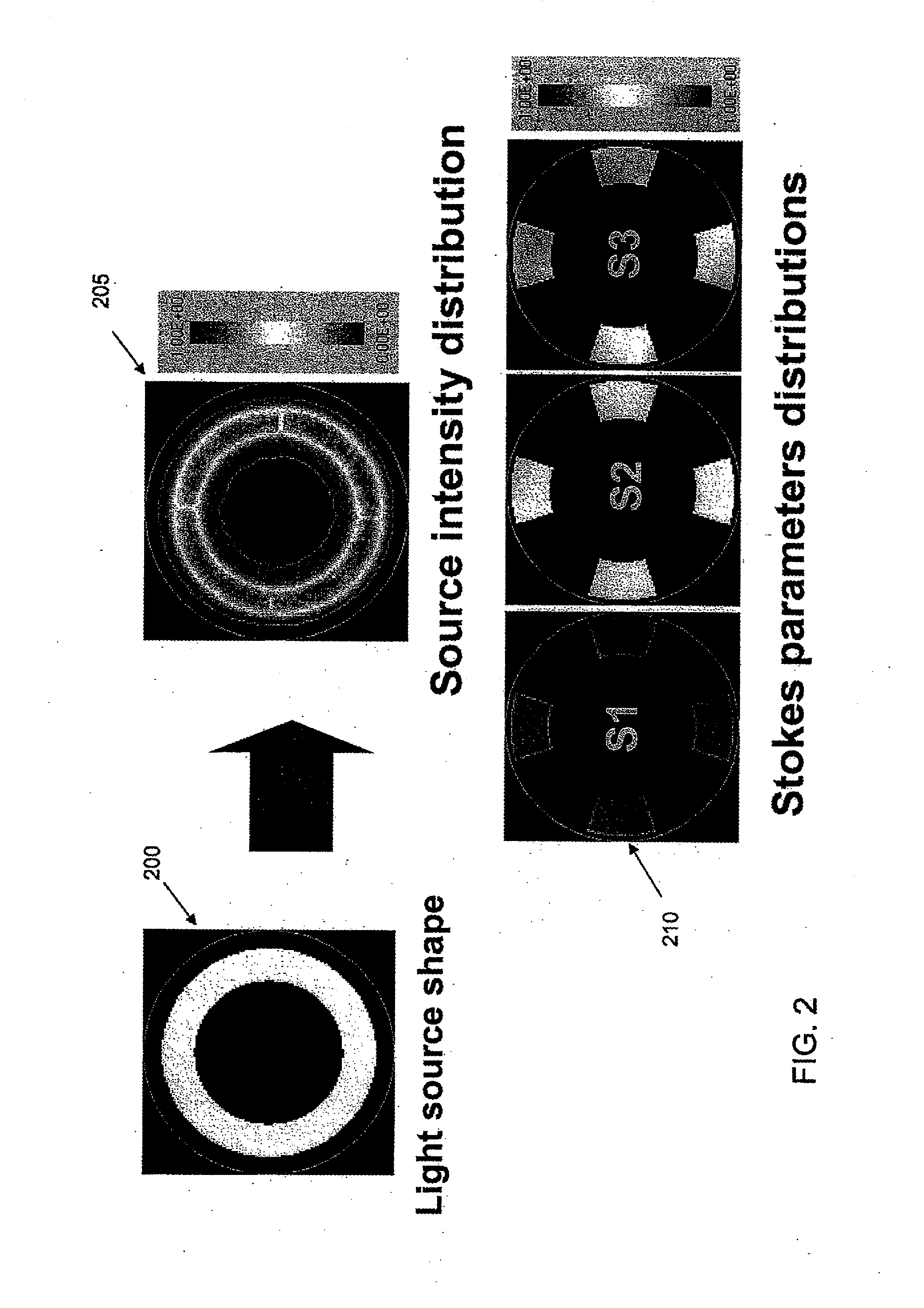
[0032]To achieve nanometer level CD control with fast turnaround time, the system and method of the invention uses more than just traditional input parameters such as lithography dose, defocus, light source type and lens parameters. For example, the simulation and modeling inputs of the invention include immersion effects, spectral bandwidth and chromatic aberrations, polarization impacts, global and local flare, wavefront aberrations, scan synchronization effec...


PUM


Abstract

A modeling technique is provided. The modeling technique includes inputting tool parameters into a model and inputting basic model parameters into the model. The technique further includes generating a simulated, corrected reticle design using the tool parameters and the basic model parameters. An image of test patterns is compared against the simulated, corrected reticle design. A determination is made as to whether δ1<ε-1, wherein δ1 represents model vs. exposure difference and ε-1 represents predetermined criteria. The technique further includes completing the model when δ1<ε-1.

Description

CROSS REFERENCE TO RELATED APPLICATIONS[0001]The present application claims priority under 35 U.S.C. §119 to U.S. Provisional Application Ser. No. 60 / 885,547, filed on Jan. 18, 2007, the contents of which are herein incorporated by reference in their entirety.FIELD OF THE INVENTION[0002]The invention generally relates to an optical proximity correction (OPC) system and method of use and, more particularly to modeling techniques used for scanner based reticle designs.BACKGROUND OF THE INVENTION[0003]Semiconductor manufacturing is limited by the lithography process, which prints increasingly finer circuit patterns. In turn, the lithography process is driven by two technologies: wafer lithography equipment and computational lithography. Historically, wafer lithography and computational lithography have been separate and independent processes, each attempting to optimize the lithography process to produce finer circuit patterns.[0004]In the current generation of microelectronics it has ...

Claims


Application Information

Patent Timeline
Patent Type & Authority Applications(United States)
IPC IPC(8): G06F17/50
CPCG03F1/144G06F17/50G03F1/36G03F1/68G06F17/5081
Inventor TYMINSKI, JACEKPOPESCU, RALUCAMATSUYAMA, TOMOYUKI
Owner NIKON CORP
Why Eureka
Try Eureka