Liquid crystal display panel

Active Publication Date: 2010-04-01
JAPAN DISPLAY WEST
View PDF3 Cites 66 Cited by
  • Summary
  • Abstract
  • Description
  • Claims
  • Application Information

AI Technical Summary

Benefits of technology

[0025]With such a configuration, the width of the upper electrode in the formed portio

Problems solved by technology

However, an electric field cannot be generated in a desired direction in both ends of the slit-shaped openings.
However, in this liquid crystal display panel, a way of disposing the slit-shaped opening when the slit-shaped opening having the “<” shape extending in the same direction as that of a signal line in a light-shielding film (black matrix) of a color filter substrate is formed in the upper electrode formed across the signal lines is not taken into consideration.
When a color filter

Method used


Image

  • Liquid crystal display panel
  • Liquid crystal display panel
  • Liquid crystal display panel

Examples


first embodiment

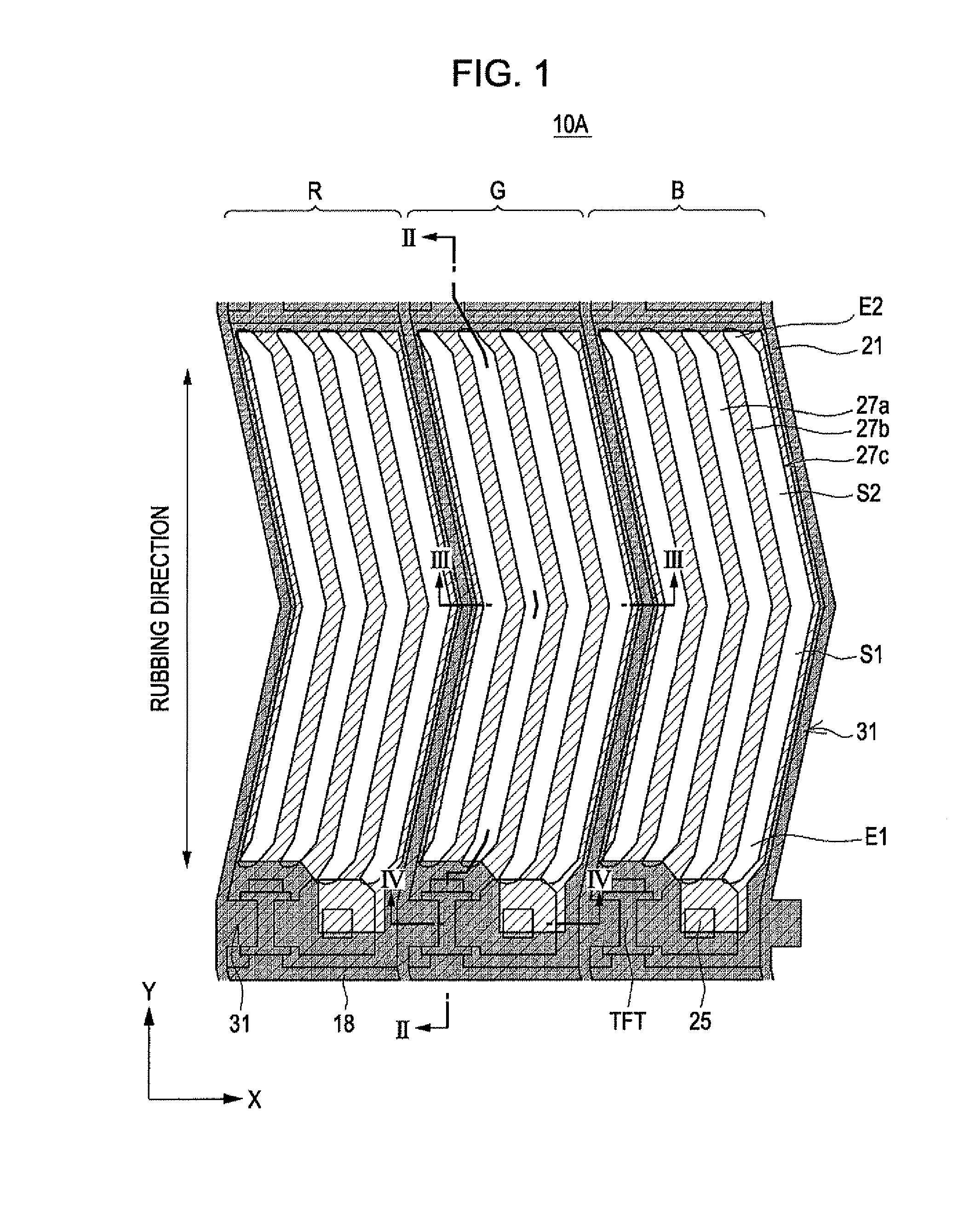
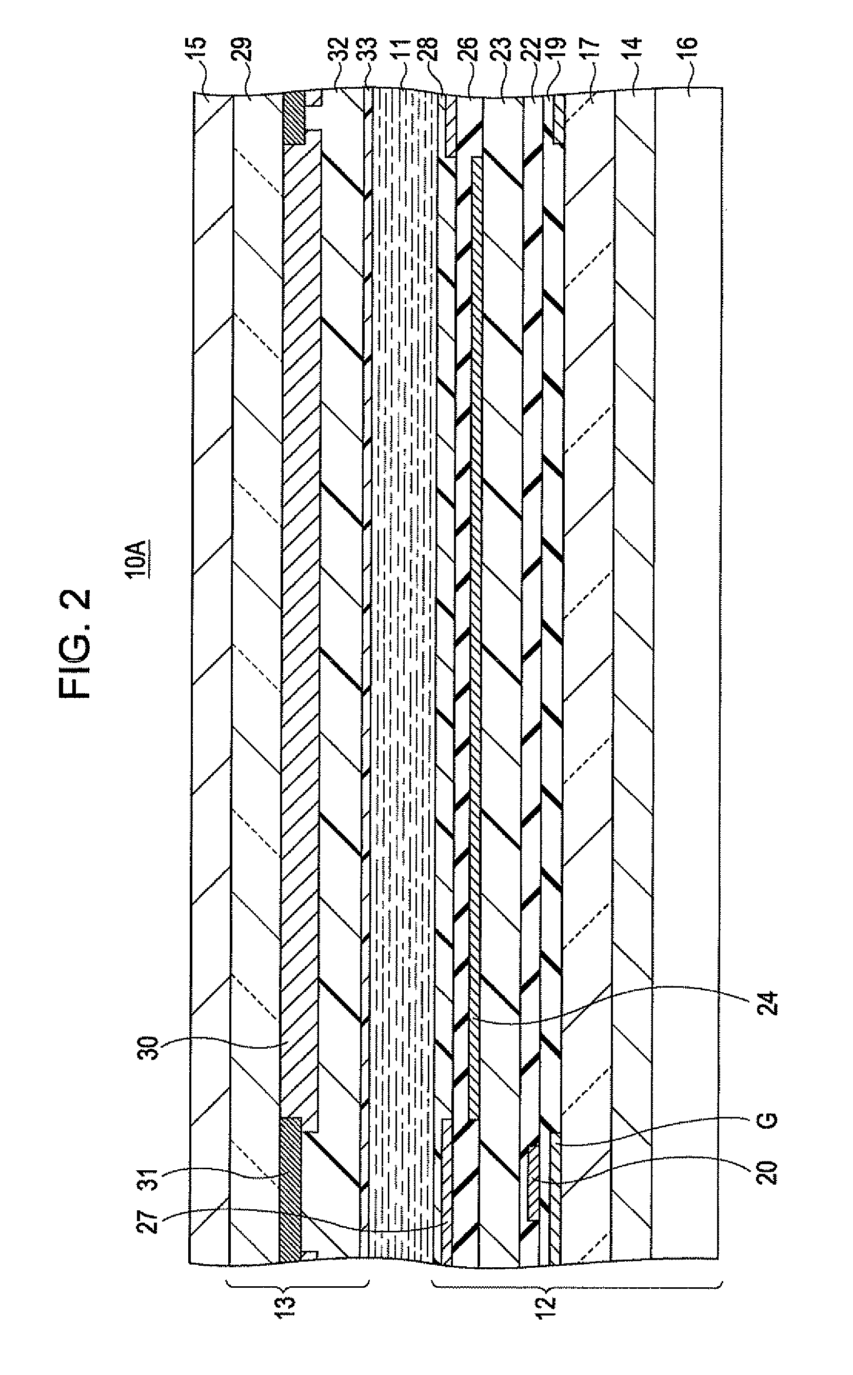
[0039]A liquid crystal display panel 10A according to the first embodiment will be described with reference to FIGS. 1 to 5. The liquid crystal display panel 10A includes an array substrate 12 and a color filter substrate 13, and a liquid crystal layer 11 interposed between the array substrate 12 and the color filter substrate 13, as shown in FIGS. 2 and 3. Even though not illustrated, the thickness of the liquid crystal layer 11 is uniformly maintained by a spacer. On the rear surface of the array substrate 12, a first polarizing plate 14 is formed. On the front surface of the color filter substrate 13, a second polarizing plate 15 is formed. On the rear surface of the array substrate 12, a backlight unit 16 emitting light is disposed.

[0040]First, the configuration of the array substrate 12 will be described. The array substrate 12 includes a substrate main body 17 as a base substrate made of a material such as glass, quartz, or plastic. On a side of the substrate main body 17 of t...

second embodiment

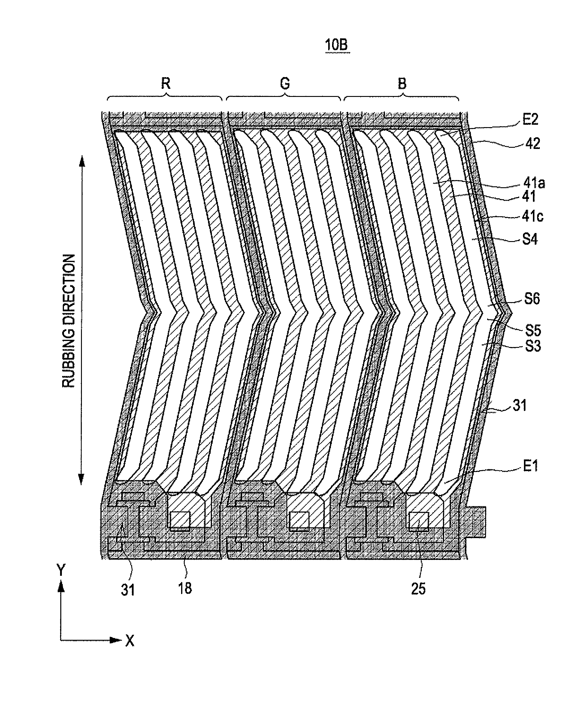
[0064]A liquid crystal display panel 10B according to a second embodiment will be described with reference to FIGS. 7 and 8. A difference between the liquid crystal display panel 10A according to the first embodiment and the liquid crystal display panel 10B according to the second embodiment is that the slit-shaped opening is formed in a double “10A according to the first embodiment. In the liquid crystal display panel 10B according to the second embodiment, the same reference numerals are given to the same constituent elements as those of the liquid crystal display panel 10A according to the first embodiment and detailed description is omitted. If necessary, FIGS. 2 to 4 are referred.

[0065]When the slit-shaped openings 27a are connected to each other, a ripple problem occurs in that domains where alignment directions are different from each other come and go in the connection portions. The configuration of the liquid crystal display panel 10B according to the second embodiment make...


PUM


Abstract

A liquid crystal display panel includes: a pair of substrates which are opposed to each other; and a liquid crystal layer which is interposed between the pair of substrates, wherein one of the pair of substrates is provided with a plurality of scanning lines and a plurality of signal lines which are arranged in a matrix shape in a display area, lower electrodes which are each formed in each of sub-pixel areas partitioned by the plurality of scanning lines and the plurality of signal lines, an insulating film which is formed in the display area so as to cover the lower electrodes, upper electrodes which are formed in the display area through the insulating film and each have a plurality of slits in each of the sub-pixel area, and an alignment film which is formed on the upper electrodes and slit-shaped openings close to the liquid crystal layer, wherein the other of the pair of substrates is provided with light-shielding films which are formed at locations overlapping with the scanning lines and the signal lines in plan view, wherein each of the upper electrodes overlaps with each of the light-shielding films in at least a partial portion in plan view, wherein each of the slit-shaped openings extends along any one of the signal line or the scanning line and has a main portion extending in an direction inclined at a predetermined angle with respect to a rubbing direction of the alignment film and a front end portion, and wherein an edge of the circumference of at least one of the slit-shaped openings formed on both sides of the light-shielding film so as to dispose the light-shielding film therebetween in plan view does not overlap with the light-shielding film disposed between the slit-shaped openings in plan view.

Description

BACKGROUND[0001]1. Technical Field[0002]The present invention relates to a transverse electric field mode liquid crystal display panel. Specifically, the present invention relates to a transverse electric mode liquid crystal display panel in which slits of an upper electrode extends along a signal line or a scanning line.[0003]2. Related Art[0004]The liquid crystal display panel has been used as a display unit in numerous electronic apparatuses since the liquid crystal display panel has features such as lightness, thinness, low power consumption in comparison to a CRT (Cathode Ray Tube). The liquid crystal display panel is a device which displays an image in such a manner that a direction of liquid crystal molecules aligned in a predetermined direction by performing a rubbing process on an alignment film is changed by an electric field and an amount of transmitted light or an amount of reflected light is varied.[0005]As a method of applying the electric field to a liquid crystal lay...

Claims


Application Information

Patent Timeline
IPC IPC(8): G02F1/1337
CPCG02F1/133512G02F2001/134372G02F1/134363G02F1/134372
Inventor TANAKA, SHINICHIRONAKANISHI, YASUHIRO
Owner JAPAN DISPLAY WEST
Why Eureka
Try Eureka