Supercharge Your Innovation With Domain-Expert AI Agents!

Integrated circuit, electronic device and ESD protection therefor

a technology of integrated circuits and electronic devices, applied in emergency protective arrangements for limiting excess voltage/current, electrical equipment, semiconductor devices, etc., can solve the problems of increasing the size and cost of esd clamps b>130/b> and isolation diodes, the amount of space they take up within the ic, and damage to ic components

Active Publication Date: 2010-05-27
NXP USA INC
View PDF11 Cites 8 Cited by
  • Summary
  • Abstract
  • Description
  • Claims
  • Application Information

AI Technical Summary

Problems solved by technology

ESD events are occurrences of high electrical potentials of limited energy that can cause damage to IC components.
This inherently increases the size and cost of the ESD clamp 130 and the isolation diodes 140, and thus the amount of space they take up within the IC 100, and thereby overall cost of the IC 100.
This has a direct impact on the size and the cost of the components, which in turn affects both the cost of the IC package, and the required footprint for the IC package on a printed circuit board or the like.
This is particularly significant as technology advances, since the ESD protection circuitry is incapable of a reduction in size in line with that of the functional circuitry of the IC.
A further problem that has been identified with the prior art ESD protection is that, due to layout constraints of circuitry within an IC package, it is generally the case that a centralised ESD clamp may not be placed close to the isolation diodes.
As will be appreciated by a skilled artisan, during an ESD gun test, the relatively high peak currents involved in the test result in significant voltage drops, across even the smallest resistances.
Consequently, the length of the metal traces between the isolation diodes and the ESD clamp on the one side, and on the other side the metal traces between the ESD clamp and the ground pin, affects the ability of the ESD protection circuitry to adequately protect an IC.
However, the pins must be compatible with the power supply rating (e.g. 0.6V), and the decoupling capacitor of the power supply generally is insufficient for high levels of ESD protection, such as those required in ESD gun testing.
Although this may save on the size and cost of the IC itself, the cost, both in terms of financial cost and space requirements, is simply passed on to the printed circuit board on which the IC is mounted.
Indeed, as pins are protected individually, a plurality of ESD protection components are required, thereby significantly increasing the cost and required area for ESD protection.

Method used


Image

  • Integrated circuit, electronic device and ESD protection therefor
  • Integrated circuit, electronic device and ESD protection therefor
  • Integrated circuit, electronic device and ESD protection therefor

Examples


Embodiment Construction

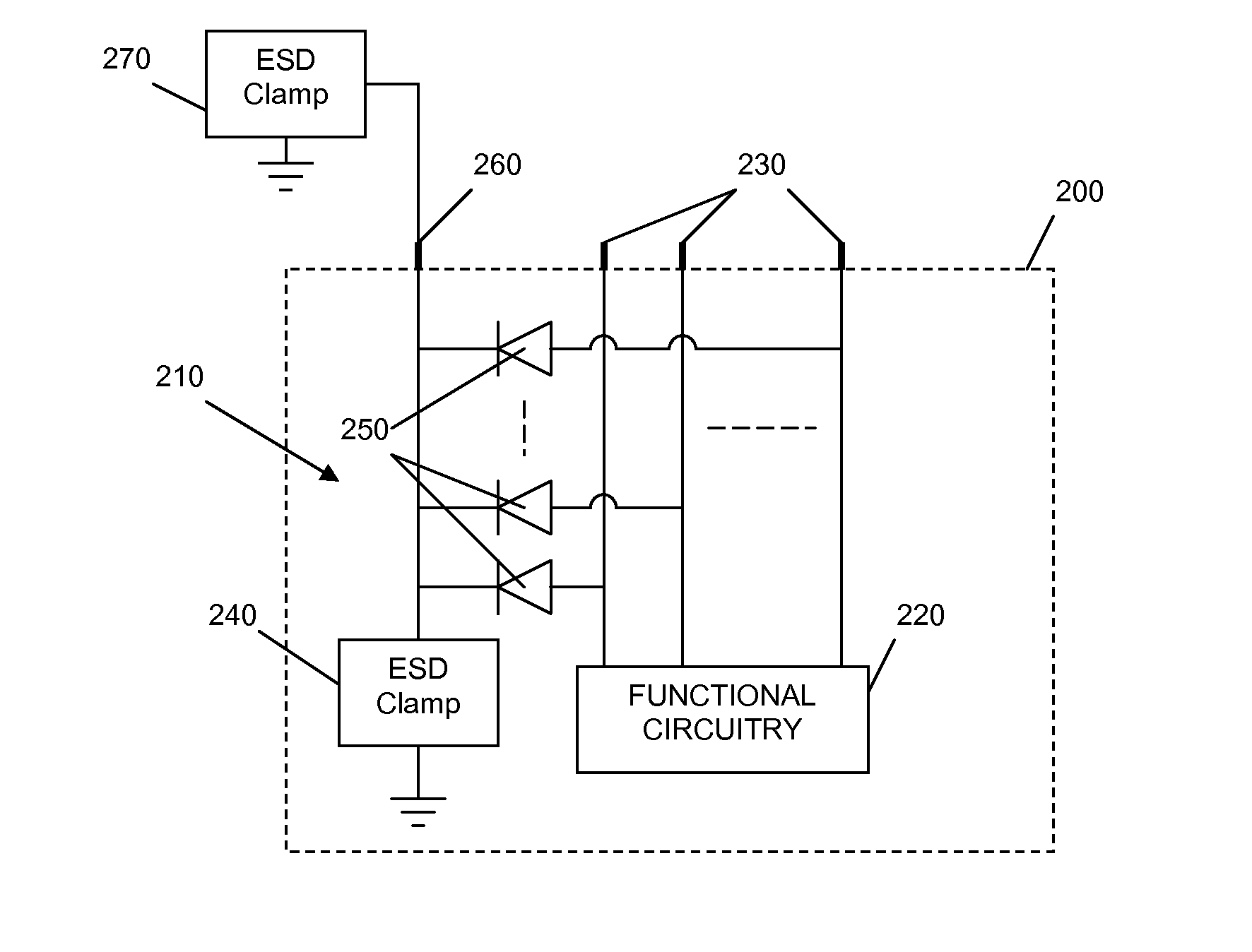
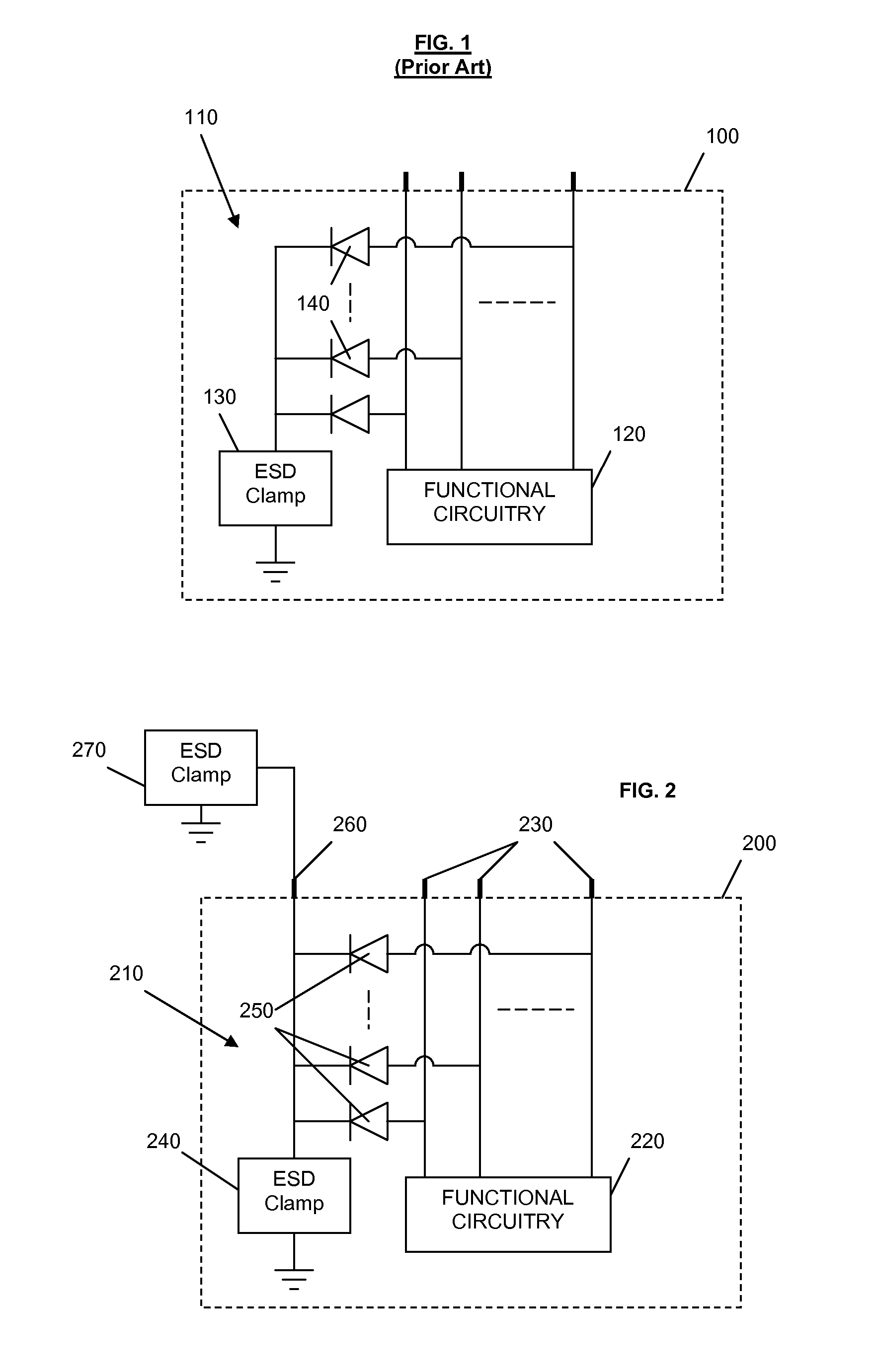
[0024]Before describing in detail embodiments that are in accordance with the invention, it should be observed that the various apparatus components described herein, and as shown in the accompanying drawings, have been represented where appropriate by conventional symbols in the drawings, showing only those specific details that are pertinent to understanding the embodiments of the present invention so as not to obscure the disclosure with details that will be readily apparent to those of ordinary skill in the art having the benefit of the description herein. Thus, it will be appreciated that for simplicity and clarity of illustration, common and well-understood elements that are useful or necessary in a commercially feasible embodiment may not be depicted in order to facilitate a less obstructed view of these various embodiments.

[0025]Referring now to FIG. 2, there is illustrated an integrated circuit (IC) 200 comprising electro-static discharge (ESD) protection circuitry 210 acco...


PUM


Abstract

An integrated circuit comprises electro-static discharge (ESD) protection circuitry arranged to provide ESD protection to one or more external connector(s) of the integrated circuit. The ESD protection circuitry comprises at least one ESD protection component coupled to the one or more external connectors for providing ESD protection thereto. The ESD protection circuitry further comprises an ESD connector, coupled to the one or more external connector(s), arranged to couple supplementary ESD protection to the one or more external connector(s).

Description

TECHNICAL FIELD[0001]The field of this invention relates to an integrated circuit, electronic device and electro-static discharge (ESD) protection therefor.BACKGROUND[0002]It is well known in the field of integrated circuit (IC) design and manufacture to provide protection to IC packages against electro-static discharge (ESD) events. ESD events are occurrences of high electrical potentials of limited energy that can cause damage to IC components.[0003]FIG. 1 illustrates an example of a known centralised ESD protection circuit 110 for an IC 100, and which forms an integrated part of the IC package.[0004]The IC 100 comprises functional circuitry 120, providing the functionality for which the IC is intended, and for which ESD protection is required. The ESD protection circuitry 110 comprises an internal ESD clamp 130, coupled to the functional circuitry 120 via isolation diodes 140. In this manner, current arising from an ESD event flows through one or more of the isolation diodes 140,...

Claims


Application Information

Patent Timeline
IPC IPC(8): H02H9/00
CPCH01L27/0251
Inventor BESSE, PATRICEHEMON, ERWANLANCE, PHILIPPE
Owner NXP USA INC
Features
  • R&D
  • Intellectual Property
  • Life Sciences
  • Materials
  • Tech Scout
  • Unparalleled Data Quality
  • Higher Quality Content
  • 60% Fewer Hallucinations
Learn More