
Solar cell and method of manufacturing the same

Inactive Publication Date: 2010-08-26
LG ELECTRONICS INC
View PDF8 Cites 0 Cited by
  • Summary
  • Abstract
  • Description
  • Claims
  • Application Information

AI Technical Summary

Benefits of technology

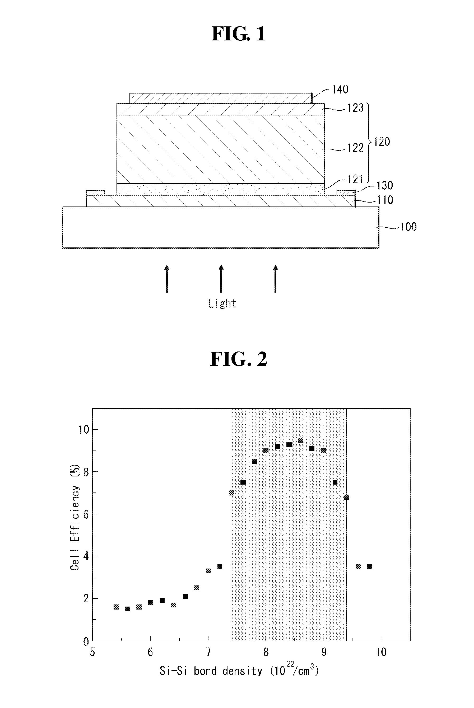
[0026]A density of Si—Si bonds in at least one of the first p-type semiconductor layer, the first n-type semiconductor layer, the second p-type semiconductor layer, and t

Problems solved by technology

While an a-Si solar cell using amorphous silicon may be manufactured as a thin solar cell, a low efficiency is obtained from the a-Si solar cell.

Method used


Image

  • Solar cell and method of manufacturing the same
  • Solar cell and method of manufacturing the same
  • Solar cell and method of manufacturing the same

Examples


Embodiment Construction

[0036]Reference will now be made in detail to embodiments of the invention, examples of which are illustrated in the accompanying drawings.

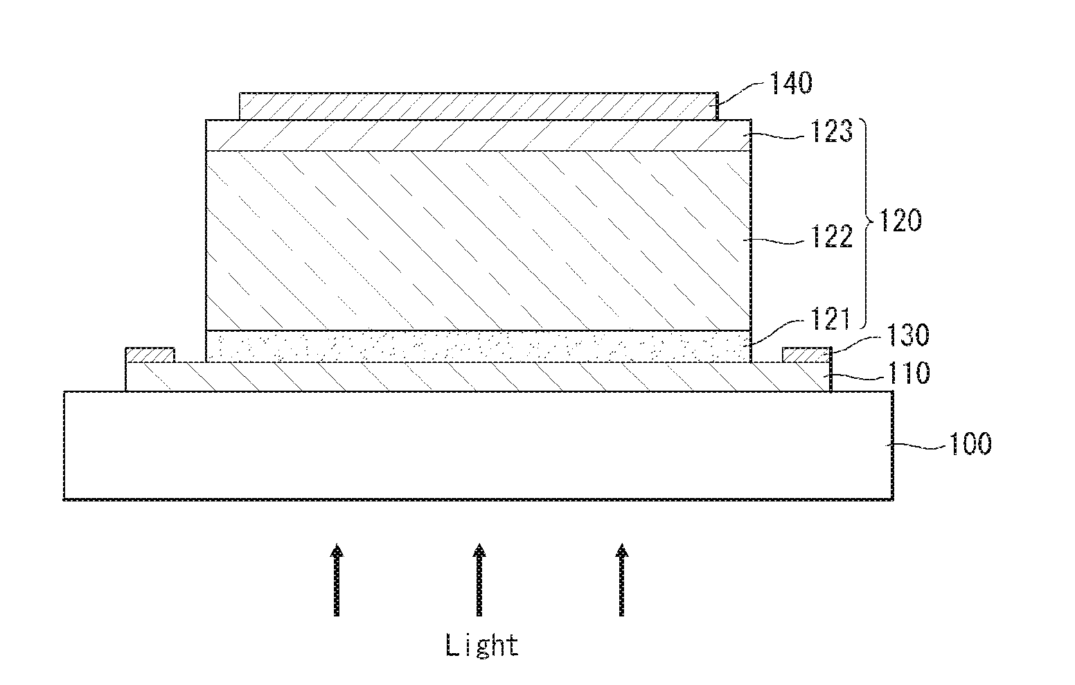
[0037]FIG. 1 illustrates an example structure of a solar cell according to an embodiment of the invention. As shown in FIG. 1, a solar cell according to an embodiment of the invention may include a substrate 100, a front electrode 110 on the substrate 100, a photoelectric conversion unit 120 and a grid electrode 130 on the front electrode 110, and a rear electrode 140 on the photoelectric conversion unit 120.

[0038]The photoelectric conversion unit 120 is positioned between the front electrode 110 and the rear electrode 140 to produce electric power using light coming from the outside. Further, the photoelectric conversion unit 120 may include an amorphous silicon layer.

[0039]The substrate 100 may provide a space for other functional layers. Further, the substrate 100 may be formed of a substantially transparent material, such as glass and plastic...


PUM


Abstract

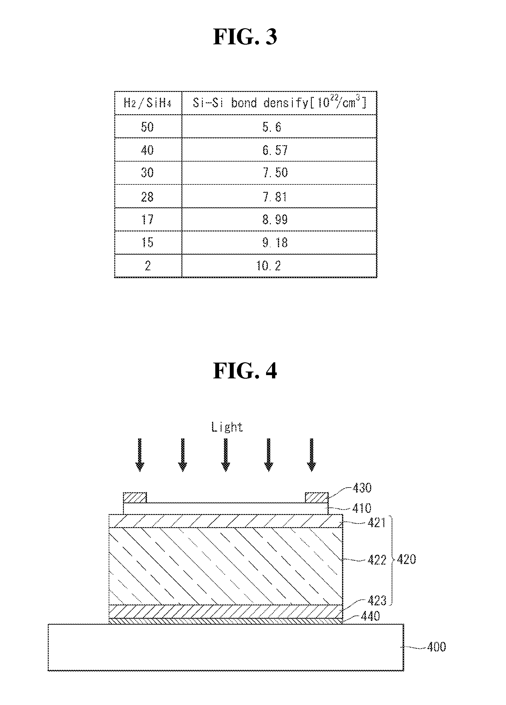
A solar cell and a method of manufacturing the same are discussed. The solar cell includes an amorphous silicon layer, and a density of Si—Si bonds in the amorphous silicon layer is 7.48×10²² / cm3 to 9.4×10²² / cm3. The method includes forming an electrode on a substrate and depositing amorphous silicon on the substrate in an atmosphere in which a ratio of an amount of hydrogen (H2) gas to an amount of silane (SiH4) gas is 15:1 to 30:1 to form an amorphous silicon layer on the substrate.

Description

[0001]This application claims the benefit of Korean Patent Application No. 10-2009-0015781 filed on Feb. 25, 2009, the entire contents of which is incorporated herein by reference for all purposes as if fully set forth herein.BACKGROUND OF THE INVENTION[0002]1. Field of the Invention[0003]Embodiments of the invention relate to a solar cell and a method of manufacturing the same.[0004]2. Discussion of the Related Art[0005]A solar cell is an element capable of converting light energy into electrical energy. The solar cell may be mainly classified into a silicon-based solar cell, a compound-based solar cell, and an organic-based solar cell depending on a material used. The silicon-based solar cell may be classified into a crystalline silicon (c-Si) solar cell and an amorphous silicon (a-Si) solar cell depending on a phase of a semiconductor. Further, the solar cell may be classified into a bulk type solar cell and a thin film type solar cell depending on a thickness of a semiconductor....

Claims


Application Information

Patent Timeline
IPC IPC(8): H01L31/00
CPCH01L31/076H01L31/1804H01L31/1824Y02E10/547Y02E10/545Y02E10/548H01L31/202Y02P70/50H01L31/04
Inventor EO, YOUNGJOOAHN, SEHWONLEE, SEUNGYOON
Owner LG ELECTRONICS INC
Learn More