Configurations and methods for manufacturing charge balanced devices

a technology of charge balanced devices and configuration methods, which is applied in the direction of semiconductor devices, basic electric elements, electrical appliances, etc., can solve the problems of limited practical applications and usefulness of high-voltage semiconductor power devices, low throughput and yield, and difficult manufacturing technology and device configuration to further increase the breakdown voltage with reduced series resistance, etc., to achieve simple and convenient processing steps, reduce processing steps, and simplify manufacturing processes

a technology of charge balanced devices and configuration methods, which is applied in the direction of semiconductor devices, basic electric elements, electrical appliances, etc., can solve the problems of limited practical applications and usefulness of high-voltage semiconductor power devices, low throughput and yield, and difficult manufacturing technology and device configuration to further increase the breakdown voltage with reduced series resistance, etc., to achieve simple and convenient processing steps, reduce processing steps, and simplify manufacturing processes

US20110001187A1Active Publication Date: 2011-01-06ALPHA & OMEGA SEMICON INC

Image

  • Configurations and methods for manufacturing charge balanced devices
  • Configurations and methods for manufacturing charge balanced devices
  • Configurations and methods for manufacturing charge balanced devices

Examples


Embodiment Construction

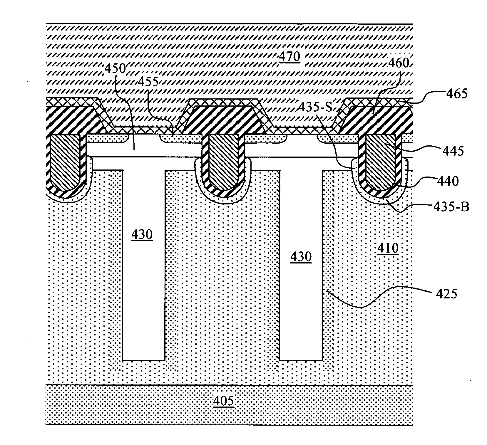
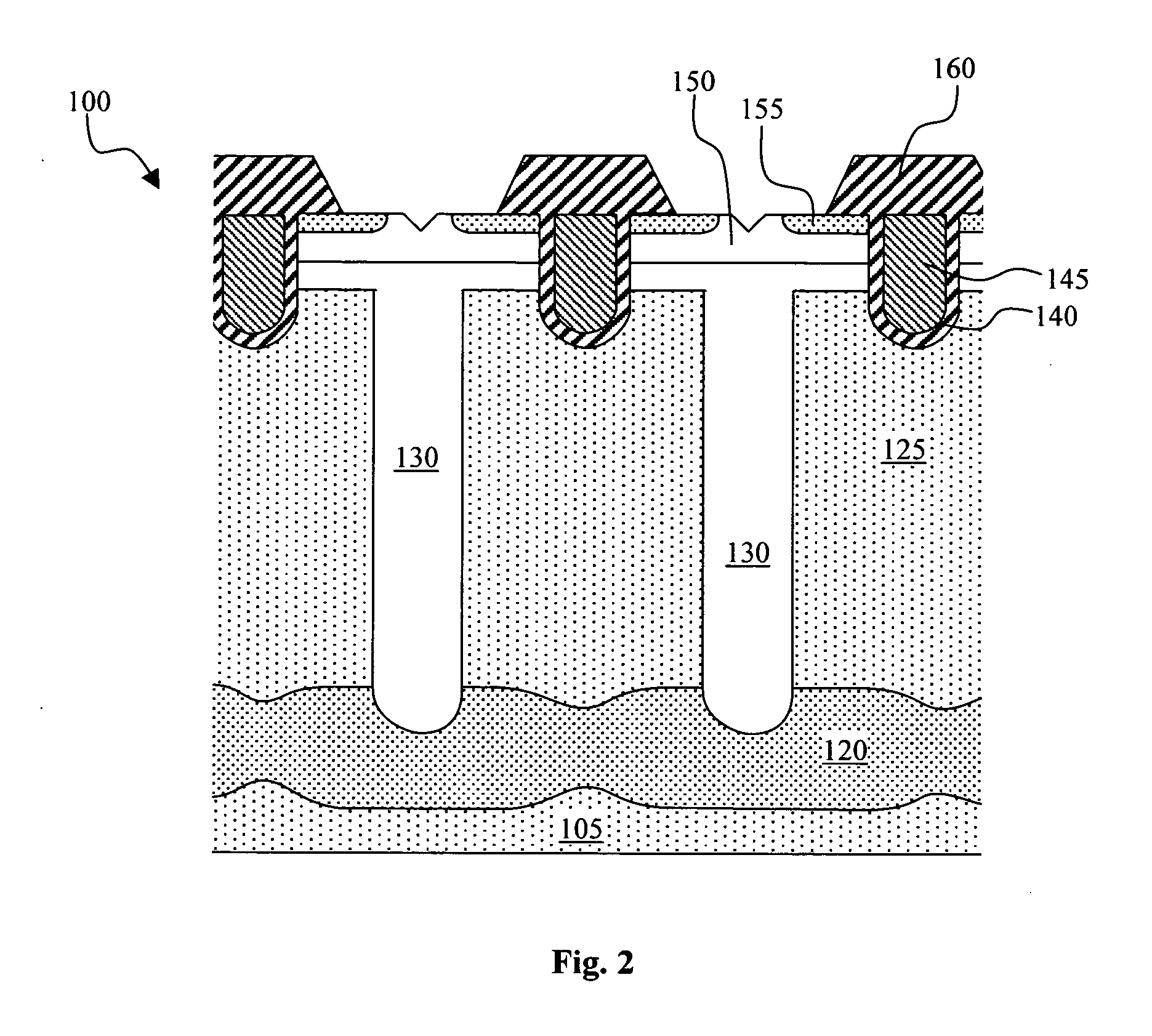
[0030]Referring to FIG. 2 for a cross sectional view of a MOSFET device 100 that illustrates the new concepts including the new structural and manufacturing features of this invention. The details of the MOSFET device 100 will be further described and explained in FIG. 3. The MOSFET device 100 is supported on an N type substrate 105 that includes a N+ doped bottom region 120 functioning as drain contact region doped through deep trenches 130 (after back grinding, as shown in FIG. 3 below) that is filled with a P-epitaxial layer therein. The MOSFET transistor cells are supported on the single thin P-epitaxial layer filling in epitaxial column trenches 130 and covering over the top surface surrounding the P-epitaxial columns that has the P-epitaxial filling in the column trenches. The thin P-epitaxial region at the top is formed with the body regions 150 surrounding the trench gate 145 filled with gate polysilicon therein. The P-body regions 150 further encompass the source regions 15...


PUM


Abstract

This invention discloses a semiconductor power device disposed in a semiconductor substrate and the semiconductor substrate has a plurality of deep trenches. The deep trenches are filled with an epitaxial layer thus forming a top epitaxial layer covering areas above a top surface of the deep trenches covering over the semiconductor substrate. The semiconductor power device further includes a plurality of transistor cells disposed in the top epitaxial layer whereby a device performance of the semiconductor power device is dependent on a depth of the deep trenches and not dependent on a thickness of the top epitaxial layer. Each of the plurality of transistor cells includes a trench DMOS transistor cell having a trench gate opened through the top epitaxial layer and filled with a gate dielectric material.

Description

[0001]This is a Divisional Application of a previously filed co-pending Application with Ser. No. 12 / 229,250 filed on Aug. 20, 2008 by identical common inventors of this Application. The disclosures made in application Ser. No. 12 / 229,250 are hereby incorporated by reference in this Patent Application.BACKGROUND OF THE INVENTION[0002]1. Field of the Invention[0003]The invention relates generally to the vertical semiconductor power devices. More particularly, this invention relates to configurations and methods implemented with a single thin epitaxial layer with improved manufacturability for manufacturing flexibly scalable charge balanced vertical semiconductor power devices with a super-junction structure with simple manufacturing processes independent of the targeted breakdown voltage.[0004]2. Description of the Prior Art[0005]Conventional manufacturing technologies and device configuration to further increase the breakdown voltage with reduced series resistance are still confront...

Claims


Application Information

Patent Timeline
06 Jan 2011
Publication
US20110001187A1
IPC
H01L29/78
CPC
H01L21/26586; H01L29/0623; H01L29/0634; H01L29/0873; H01L29/7813; H01L29/1095; H01L29/41766; H01L29/4236
Inventors
HEBERT, FRANCOIS