Touch Panel and Display Apparatus

a display apparatus and touch panel technology, applied in the field of touch panels, can solve the problems of cracks in the touch substrate, easy to cause reflected glare (external light reflection) in the touch panel, and the touch substrate may become relatively weak, so as to reduce reflected glare and improve reliability.

Inactive Publication Date: 2011-03-24
KYOCERA CORP
View PDF12 Cites 18 Cited by
  • Summary
  • Abstract
  • Description
  • Claims
  • Application Information

AI Technical Summary

Benefits of technology

It is an object of the present invention to provide a touch panel that reduces reflected glare and improves reliability.
In the touch panel according to one embodiment of the present invention, there exists the light diffusing particles and the recesses in the first substrate. As a result, the reflected glare can be reduced. Further, in the touch panel, at least some of the light diffusing particles are arranged in the recesses of the first substrate. As a result, the pressing force that acts on the first substrate when the first substrate is deformed by a pressing operation is dispersed, and concentration of the stress at corners of the recesses can be eased. Therefore, in the touch panel, reflected glare can be reduced and reliability can be improved.
The touch panel type display device according to an embodiment of the present invention includes the touch panel. Therefore, the same effect as that of the above-described touch panel can be achieved. That is, in the touch panel type display device, reflected glare can be reduced and reliability can be improved.

Problems solved by technology

However, reflected glare (external light reflection) may be easily caused in the touch panel.
However, if the technique of forming the minute unevenness in the touch substrate is applied, the touch substrate may become relatively weak as compared with the case where the minute unevenness is not formed.
For this reason, when the touch substrate is pressed and deformed, cracks may occur in the touch substrate and the touch substrate may easily be damaged.
As a result, reliability of the touch panel may be lowered.

Method used


Image

  • Touch Panel and Display Apparatus
  • Touch Panel and Display Apparatus
  • Touch Panel and Display Apparatus

Examples


Embodiment Construction

Hereinafter, a touch panel and a touch panel type display device according to an embodiment of the present invention will be described with reference to the drawings.

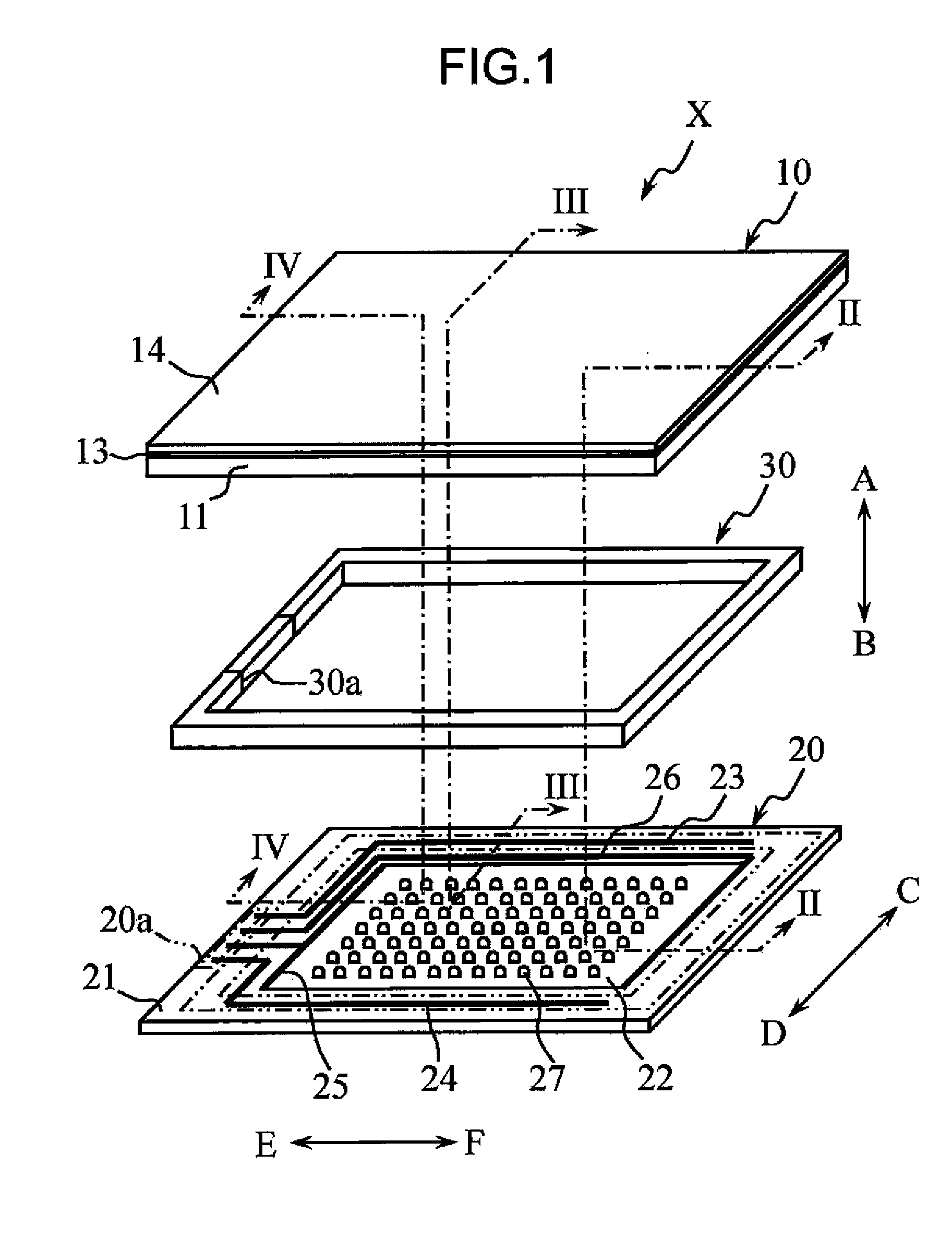
First, a touch panel according to an embodiment of the present invention will be described with reference to FIGS. 1 to 4.

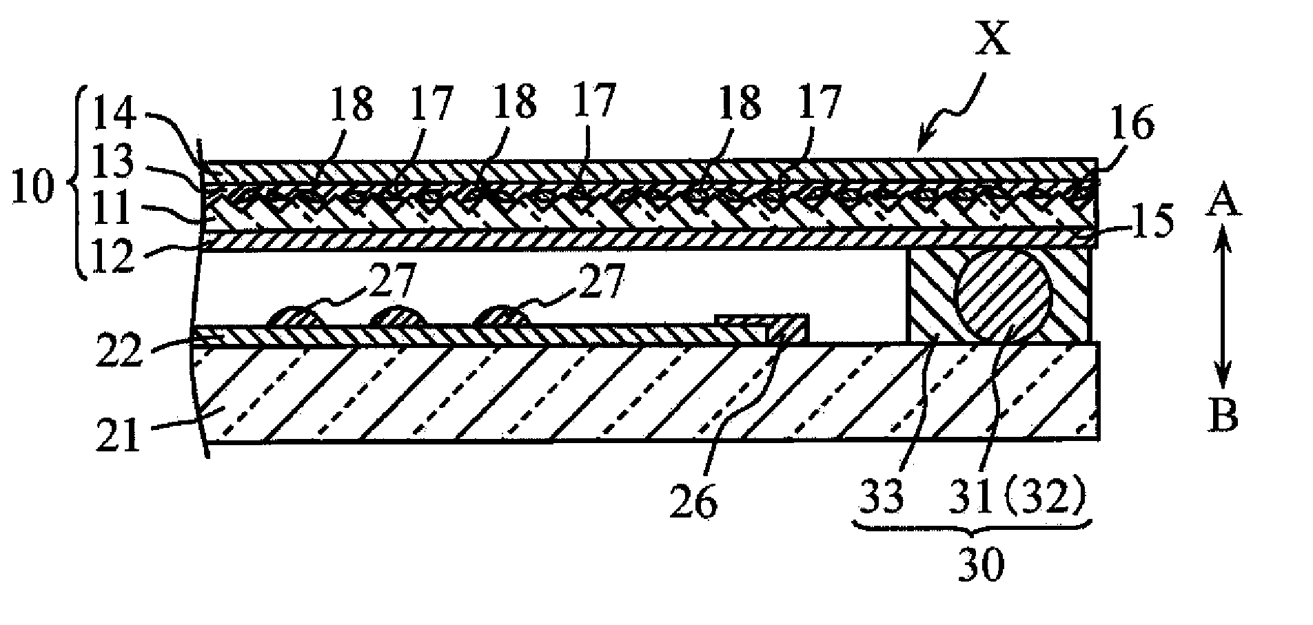
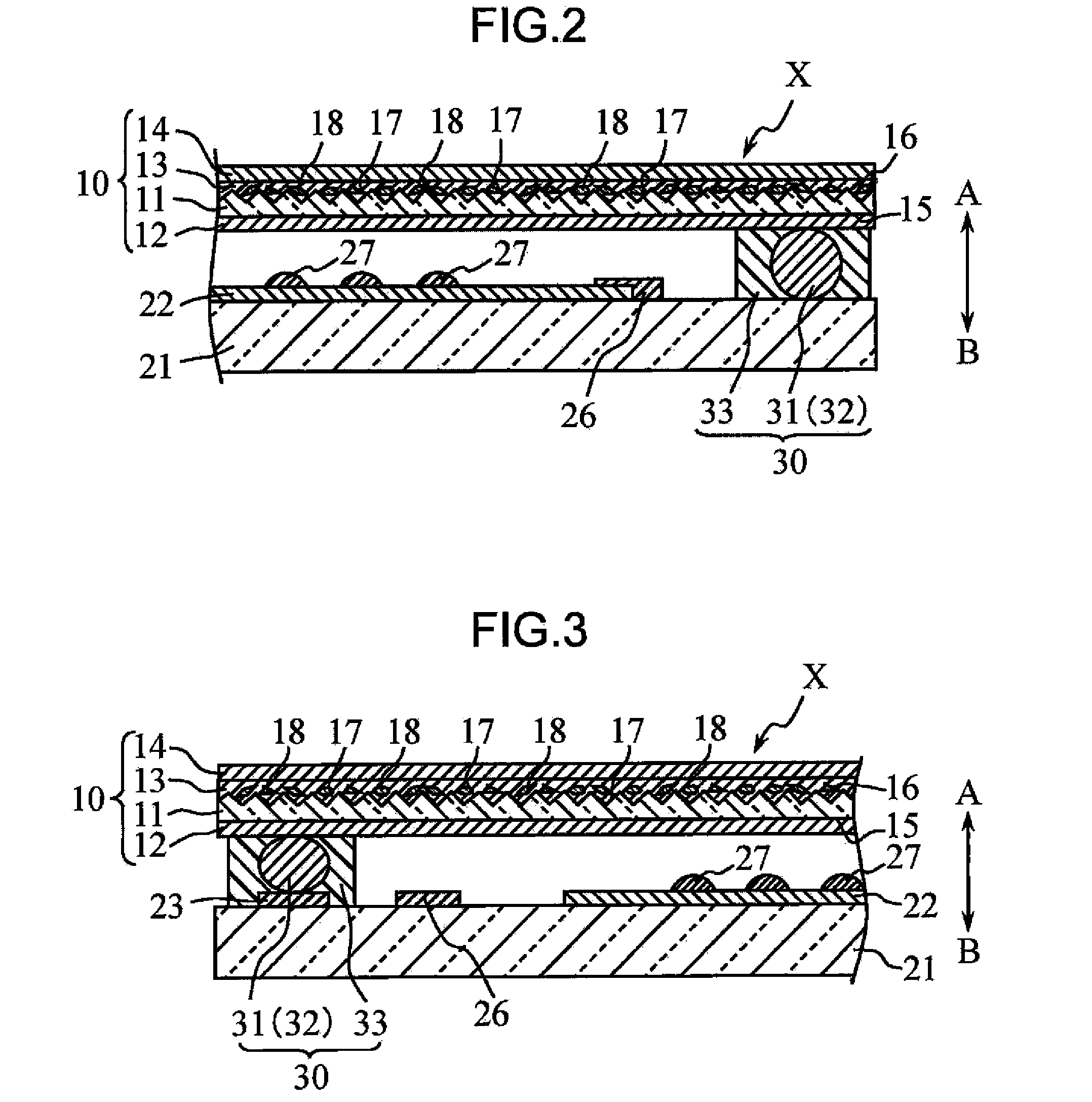
A touch panel X includes a first base 10, a second base 20, and a conductive adhesive member 30.

The first base 10 includes a transparent insulating substrate 11 (first substrate), a transparent electrode 12, an adhesive member 13, and a polarizing film (optical film) 14, and is flexible as a whole. The first base 10 has a substantially rectangular shape in plan view. However, the shape of the first base 10 in plan view is not limited to the rectangular shape.

The transparent insulating substrate 11 performs a function of supporting the transparent electrode 12 and has a sufficient electric insulating property. The transparent insulating substrate 11 has a first principal surface 15 that faces the seco...


PUM


Abstract

According to one embodiment, a touch panel includes: a first substrate, a second substrate, and at least one light diffusing particle. The first substrate includes a first principal surface, a second principal surface positioned at a side opposite to the first principal surface, and at least one recess on the second principal surface. The second substrate is arranged to face the first principal surface. At least a portion of the light diffusing particle is positioned corresponding to the recess.

Description

TECHNICAL FIELDThe present invention relates to a touch panel that is disposed on a display screen such as a liquid crystal display. Further, the present invention relates to a touch panel type display device including the touch panel.BACKGROUND ARTAs an example of a screen input type display device, a display device including a touch panel is known. The touch panel is configured to detect input coordinates on the basis of a change in resistance by, for example, a pressing operation. Some touch panels have a structure in which transparent conductive films of an upper substrate and a lower substrate, respectively, are arranged to face each other.In recent years, in terms of increasing the image definition and improving durability, there is proposed a touch panel that has an upper substrate made of glass, as disclosed in Japanese: Laid-open Patent Publication No. 09-146707. This touch panel is superior to a touch panel having an upper substrate made of a resin film, in terms of an ima...

Claims


Application Information

Patent Timeline
Patent Type & Authority Applications(United States)
IPC IPC(8): G06F3/041
CPCG02F1/13338G06F3/045G06F3/0412
Inventor NOZAWA, JUNICHI
Owner KYOCERA CORP
Why Eureka
Try Eureka