Solid-state image pickup device

a solid-state image and pickup device technology, applied in the direction of color television details, television systems, radio control devices, etc., can solve the problems of deteriorating image quality, difficult for incident light to reach the photoelectric conversion region, and difficult for the amplifying solid-state image pickup device to obtain excellent sensitivity characteristics, etc., to achieve suppressed sensitivity shading

Inactive Publication Date: 2011-04-07
PANASONIC CORP
View PDF5 Cites 39 Cited by
  • Summary
  • Abstract
  • Description
  • Claims
  • Application Information

AI Technical Summary

Benefits of technology

[0018]Therefore, an object of the present invention is to provide a solid-state image pickup device in which sensitivity shading is suppressed.
[0039]The solid-state image pickup device according to the present invention can suppress sensitivity shading caused by a reduction in an amount of incident light to the peripheral portion of the pixel array region. In addition, the solid-state image pickup device according to the present invention can be manufactured by using a fabrication process similar to that of the conventional solid-state image pickup device, thereby making it unnecessary to add a new fabrication process.

Problems solved by technology

In general, it is difficult for the amplifying solid-state image pickup device to obtain more excellent sensitivity characteristics than those obtained by the CCD solid-state image pickup device.
However, the metal wires block light and make it hard for incident light to reach the photoelectric conversion region.
Accordingly, due to causes such as light blocking by the metal film, it is made hard for light to reach the photoelectric conversion region in the pixel in the peripheral portion of the pixel array, thereby causing a problem of deteriorating image quality.
However, the conventional shrink method may have difficulties in optimizing positions (i.e., displacement amounts) of the microlenses for all pixels in accordance with light incidence characteristics of the camera lens.
Therefore, in the solid-state image pickup device of the conventional art, the greater a distance between a pixel and the center of the pixel array is, the less sufficient an amount of the incident light entering into the pixel becomes, thereby causing deterioration in image quality (sensitivity shading) due to a difference between the amount of the incident light entering into the pixel in the central portion of the pixel array and the amount of the incident light entering into the pixel in the peripheral portion of the pixel array.

Method used


Image

  • Solid-state image pickup device
  • Solid-state image pickup device
  • Solid-state image pickup device

Examples


first embodiment

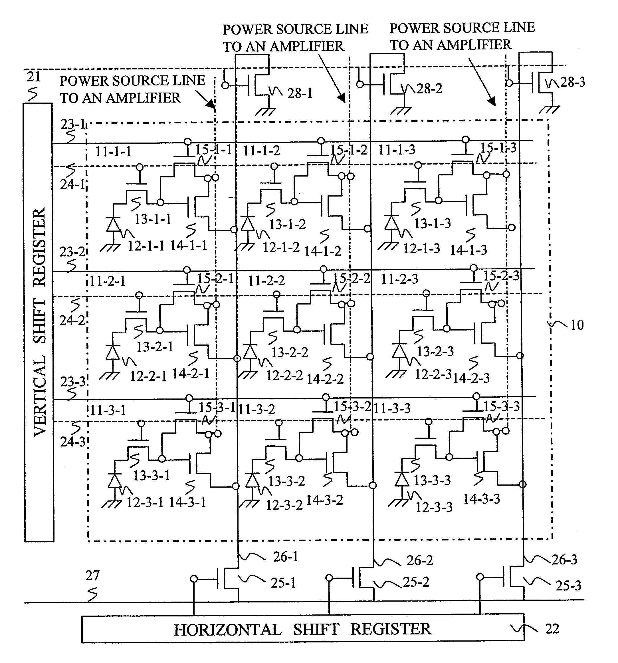
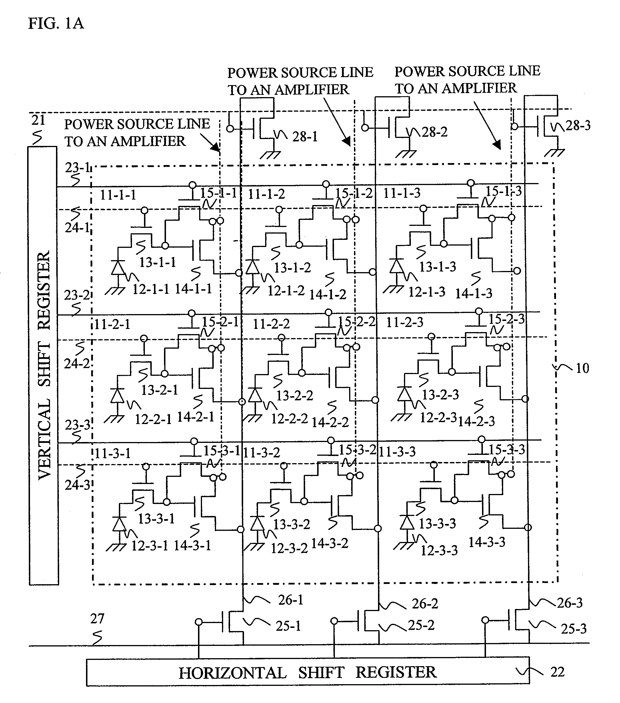
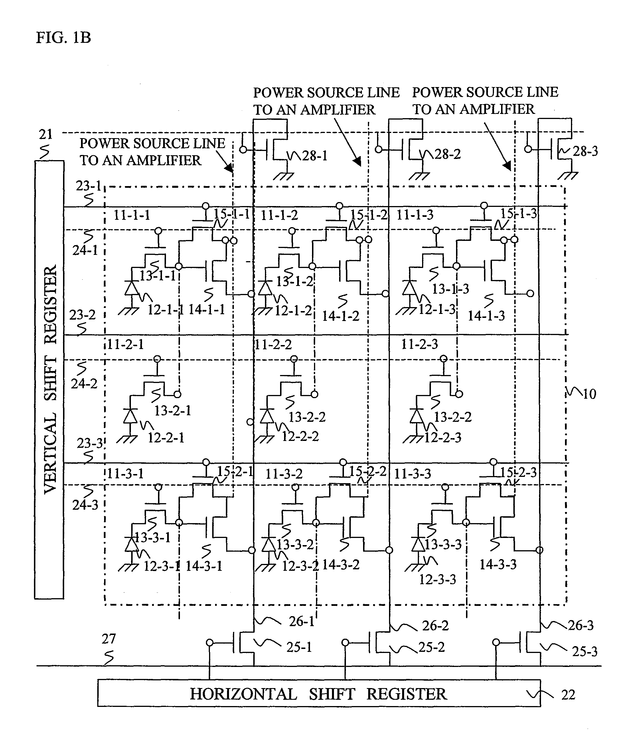
[0076]FIG. 1A is a diagram illustrating one example of a circuit configuration of a solid-state image pickup device according to a first embodiment of the present invention, and FIG. 1B is a diagram illustrating another example of a circuit configuration of a solid-state image pickup device according to the first embodiment of the present invention.

[0077]The solid-state image pickup device according to the first embodiment includes a pixel array region 10 in which a plurality of pixels including photodiodes (12-1-1 to 12-3-1) are disposed in a two-dimensional matrix manner. In FIGS. 1A and 1B, only a part of the plurality of pixels included in the pixel array region 10 is shown.

[0078]FIG. 1A is a diagram illustrating a solid-state image pickup device having a “one pixel to one cell” configuration in which one pixel is included in one cell. In the solid-state image pickup device shown in FIG. 1A, one pixel includes, for example, a photodiode 12-1-1, a transfer transistor 13-1-1, a re...

second embodiment

[0129]FIG. 5A is a schematic diagram illustrating a layout of microlenses 109 in a solid-state image pickup device according to a second embodiment and FIG. 5B is a diagram illustrating an enlarged view of the portion “Q” shown in FIG. 5A. FIG. 6 is a diagram illustrating a cross-sectional view of a pixel disposed in a central portion of a pixel array region.

[0130]Since a circuit configuration of the solid-state image pickup device according to the present embodiment is same as that of the solid-state image pickup device according to the first embodiment shown in FIGS. 1A and 1B, descriptions on the circuit configuration will be omitted here.

[0131]The solid-state image pickup device according to the present embodiment has a structure similar to that of the solid-state image pickup device according to the first embodiment shown in FIG. 1D, except displacement amounts of microlenses 109, color filters 107, and second metal films 106. In other words, as shown in FIGS. 1D and 6, pixels ...

third embodiment

[0165]Hereinafter, a solid-state image pickup device according to a third embodiment of the present invention will be described.

[0166]Since a circuit configuration of the solid-state image pickup device according to the present embodiment is same as that of the solid-state image pickup device according to the first embodiment shown in FIGS. 1A and 1B, descriptions on the circuit configuration will be omitted here.

[0167]A structure of the solid-state image pickup device according to the present embodiment is same as that of the solid-state image pickup device according to the first embodiment shown in FIG. 1D, except displacement amounts of microlenses 109, color filters 107, and second metal films 106. In other words, as shown in FIG. 1D, pixels are formed on a surface of a semiconductor substrate 101, each of which includes a photodiode 110 serving as a photoelectric conversion region, an insulating film 102 formed so as to cover a surface of the photodiode 110, a first metal film ...


PUM


Abstract

In a solid-state image pickup device, it is difficult to match an optimum incidence angle corresponding to an image height of a pixel array region with light incidence characteristics of a camera lens, thereby causing image quality deterioration due to sensitivity shading. Respective microlenses are disposed in a two-dimensional manner, i.e., in a row and a column directions. In particular, the microlenses are disposed such that each side of a disposition region where the microlenses are disposed has a concave curve with respect to a line connecting adjacent vertexes of the disposition region. In other words, a distance AH (AV) between center points of a pair of facing sides of the disposition region is set to be smaller than a distance BH (BV) between neighboring vertexes of the disposition region.

Description

BACKGROUND OF THE INVENTION[0001]1. Field of the Invention[0002]The present invention relates to a solid-state image pickup device and more particularly, to a solid-state image pickup device in which shading is suppressed.[0003]2. Description of the Background Art[0004]Conventionally, as a solid-state image pickup device, an amplifying solid-state image pickup device and a CCD solid-state image pickup device have been well-known. In general, it is difficult for the amplifying solid-state image pickup device to obtain more excellent sensitivity characteristics than those obtained by the CCD solid-state image pickup device. The reason is as follows. To supply voltages to MOS-FETs in charge detection regions, the amplifying solid-state image pickup device requires a plurality of layers (two or more layers) of metal wires above a photoelectric conversion region. However, the metal wires block light and make it hard for incident light to reach the photoelectric conversion region.[0005]FI...

Claims


Application Information

Patent Timeline
Patent Type & Authority Applications(United States)
IPC IPC(8): H04N5/335
CPCH04N5/335H04N25/00H01L27/146
Inventor KATSUNO, MOTONARIMIYAGAWA, RYOHEI
Owner PANASONIC CORP
Why Eureka
Try Eureka