Solid-state image pickup device
a solid-state image and pickup device technology, applied in the direction of radio frequency controlled devices, instruments, color signal processing circuits, etc., can solve the problems of deteriorating image quality, difficult for incident light to reach the photoelectric conversion region, and difficult for the amplifying solid-state image pickup device to obtain excellent sensitivity characteristics, etc., to achieve suppressed sensitivity shading
- Summary
- Abstract
- Description
- Claims
- Application Information
AI Technical Summary
Benefits of technology
Problems solved by technology
Method used
Image
Examples
first embodiment
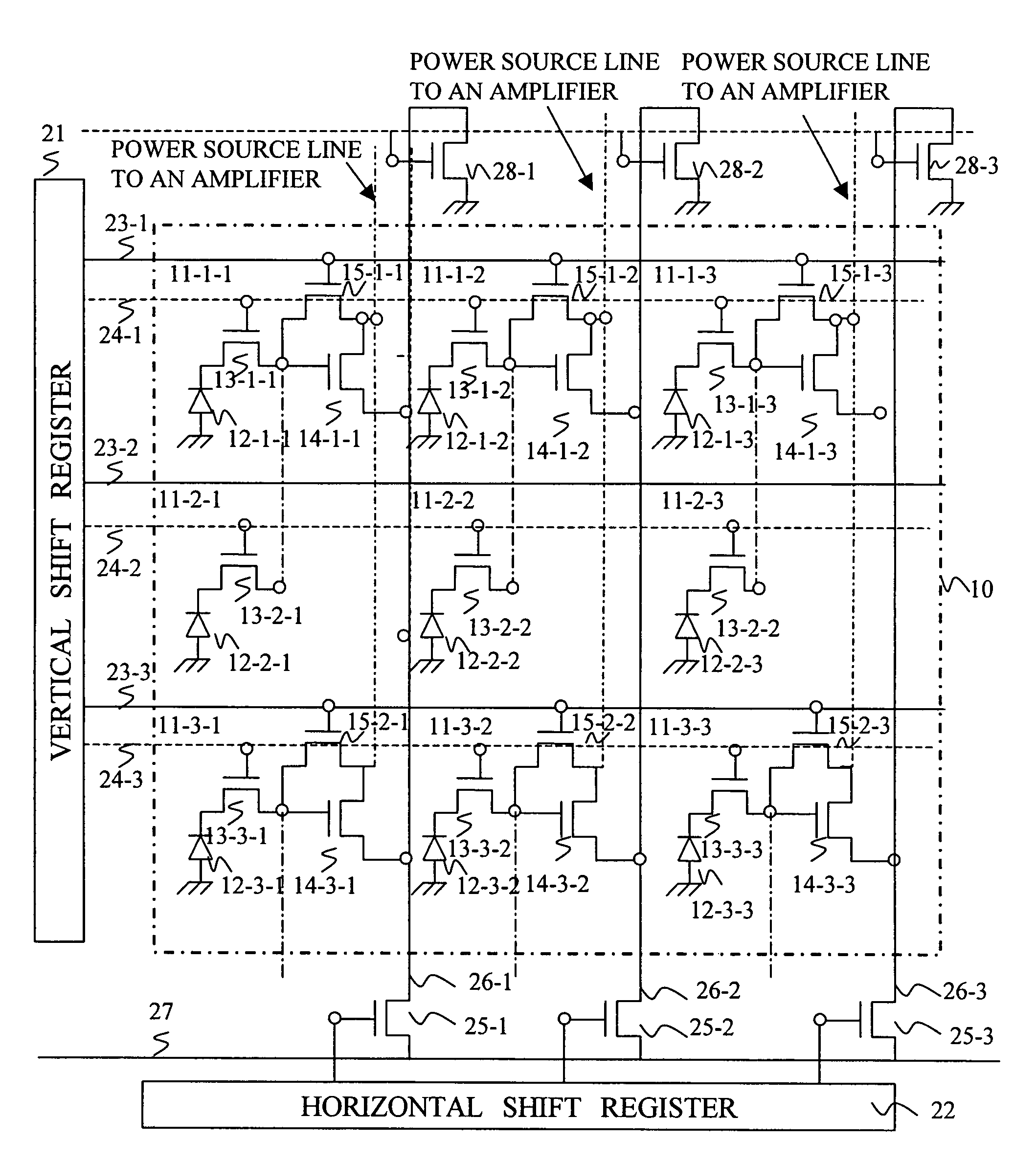
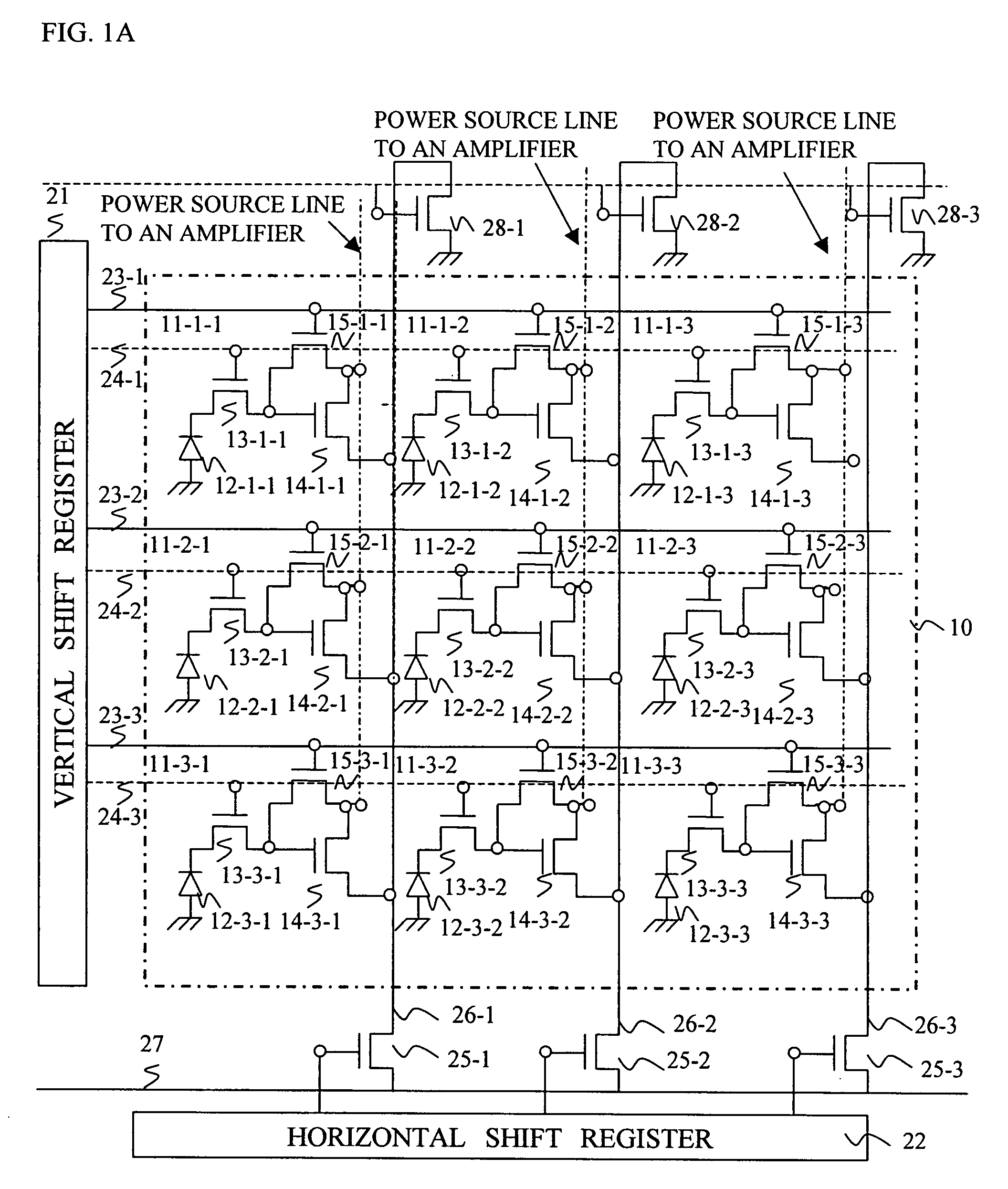
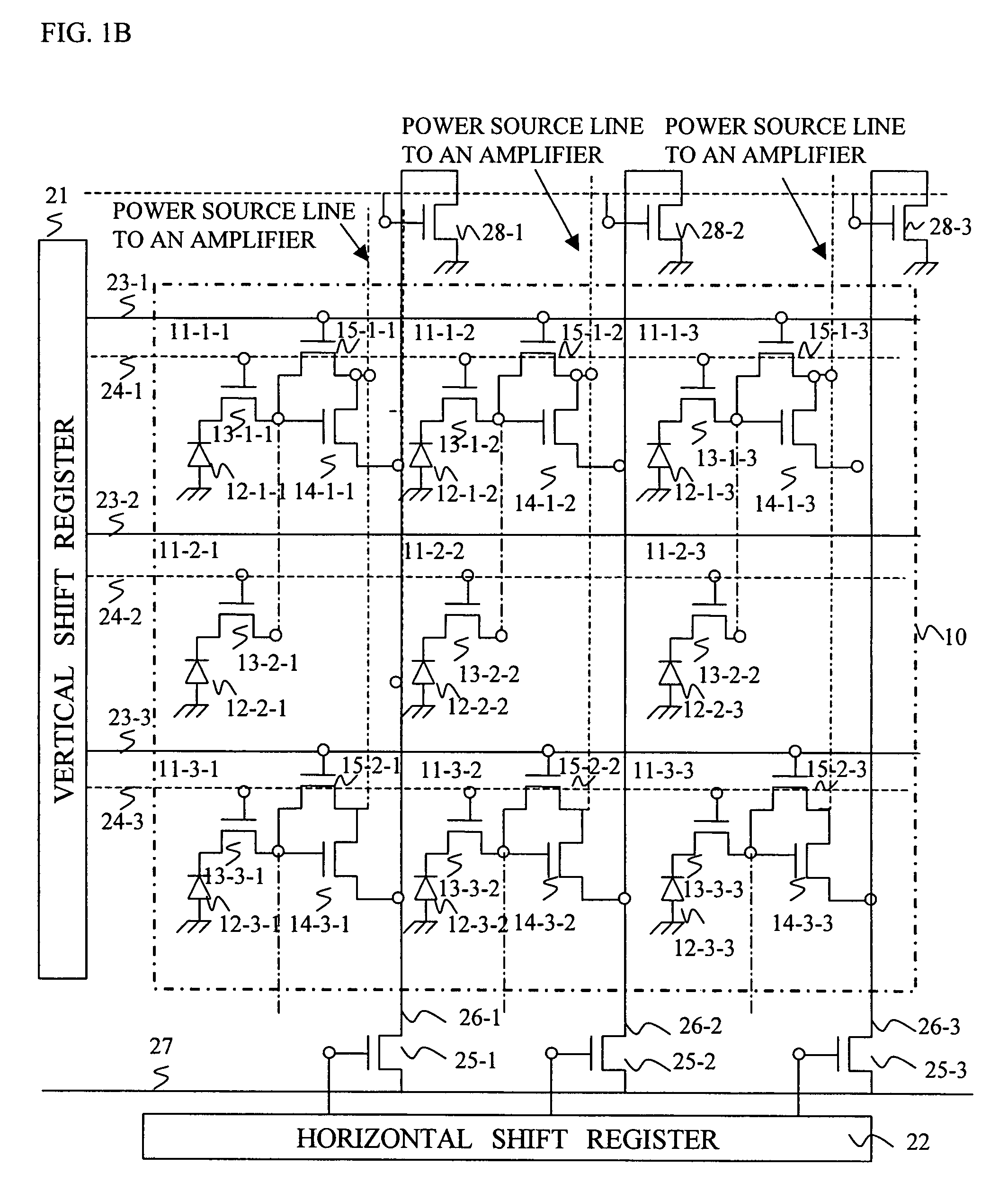
[0076]FIG. 1A is a diagram illustrating one example of a circuit configuration of a solid-state image pickup device according to a first embodiment of the present invention, and FIG. 1B is a diagram illustrating another example of a circuit configuration of a solid-state image pickup device according to the first embodiment of the present invention.
[0077]The solid-state image pickup device according to the first embodiment includes a pixel array region 10 in which a plurality of pixels including photodiodes (12-1-1 to 12-3-1) are disposed in a two-dimensional matrix manner. In FIGS. 1A and 1B, only a part of the plurality of pixels included in the pixel array region 10 is shown.
[0078]FIG. 1A is a diagram illustrating a solid-state image pickup device having a “one pixel to one cell” configuration in which one pixel is included in one cell. In the solid-state image pickup device shown in FIG. 1A, one pixel includes, for example, a photodiode 12-1-1, a transfer transistor 13-1-1, a re...
second embodiment
[0129]FIG. 5A is a schematic diagram illustrating a layout of microlenses 109 in a solid-state image pickup device according to a second embodiment and FIG. 5B is a diagram illustrating an enlarged view of the portion “Q” shown in FIG. 5A. FIG. 6 is a diagram illustrating a cross-sectional view of a pixel disposed in a central portion of a pixel array region.
[0130]Since a circuit configuration of the solid-state image pickup device according to the present embodiment is same as that of the solid-state image pickup device according to the first embodiment shown in FIGS. 1A and 1B, descriptions on the circuit configuration will be omitted here.
[0131]The solid-state image pickup device according to the present embodiment has a structure similar to that of the solid-state image pickup device according to the first embodiment shown in FIG. 1D, except displacement amounts of microlenses 109, color filters 107, and second metal films 106. In other words, as shown in FIGS. 1D and 6, pixels ...
third embodiment
[0165]Hereinafter, a solid-state image pickup device according to a third embodiment of the present invention will be described.
[0166]Since a circuit configuration of the solid-state image pickup device according to the present embodiment is same as that of the solid-state image pickup device according to the first embodiment shown in FIGS. 1A and 1B, descriptions on the circuit configuration will be omitted here.
[0167]A structure of the solid-state image pickup device according to the present embodiment is same as that of the solid-state image pickup device according to the first embodiment shown in FIG. 1D, except displacement amounts of microlenses 109, color filters 107, and second metal films 106. In other words, as shown in FIG. 1D, pixels are formed on a surface of a semiconductor substrate 101, each of which includes a photodiode 110 serving as a photoelectric conversion region, an insulating film 102 formed so as to cover a surface of the photodiode 110, a first metal film ...
PUM
 Abstract
Description
Claims
Application Information


