Solid-state imaging device

a solid-state imaging and imaging device technology, applied in the field of solid-state imaging devices, can solve problems such as sensitivity shading, and achieve the effects of suppressing sensitivity shading, reducing sensitivity shading at the periphery of imaging area, and high performan

Inactive Publication Date: 2006-08-31
COLLABO INNOVATIONS INC
View PDF19 Cites 15 Cited by
  • Summary
  • Abstract
  • Description
  • Claims
  • Application Information

AI Technical Summary

Benefits of technology

[0029] This structure enables sensitivity shading at the periphery of the imaging area to be reduced.
[0030] According to the present invention, a high performance, high-reliability solid-state imaging device is obtained that can suppress sensitivity shading by reducing the amount of shading around pixel arrays, and provide excellent connectivity between lower and upper layer wiring.
[0031] Furthermore, this solid-state imaging device can be manufactured using processes similar to a conventional structure, thereby removing the need for additional manufacturing processes, which is advantageous in terms of cost.

Problems solved by technology

The incident light thus has difficulty reaching photodiode 210, resulting in sensitivity shading.

Method used


Image

  • Solid-state imaging device
  • Solid-state imaging device
  • Solid-state imaging device

Examples


embodiment 1

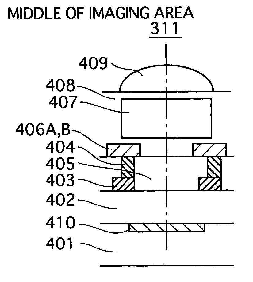
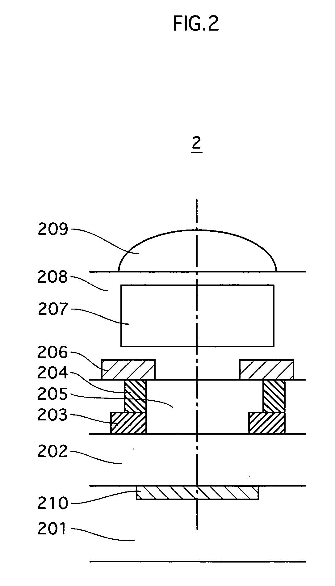
[0045] A MOS image sensor pertaining to an embodiment 1 of the present invention is characterized in that the position and shape of a metal layer in each pixel cell varies depending on the location of the pixel cell in an imaging area, so as to increase the amount of external light incident on a photodiode.

[0046] (1) Structure of MOS Image Sensor

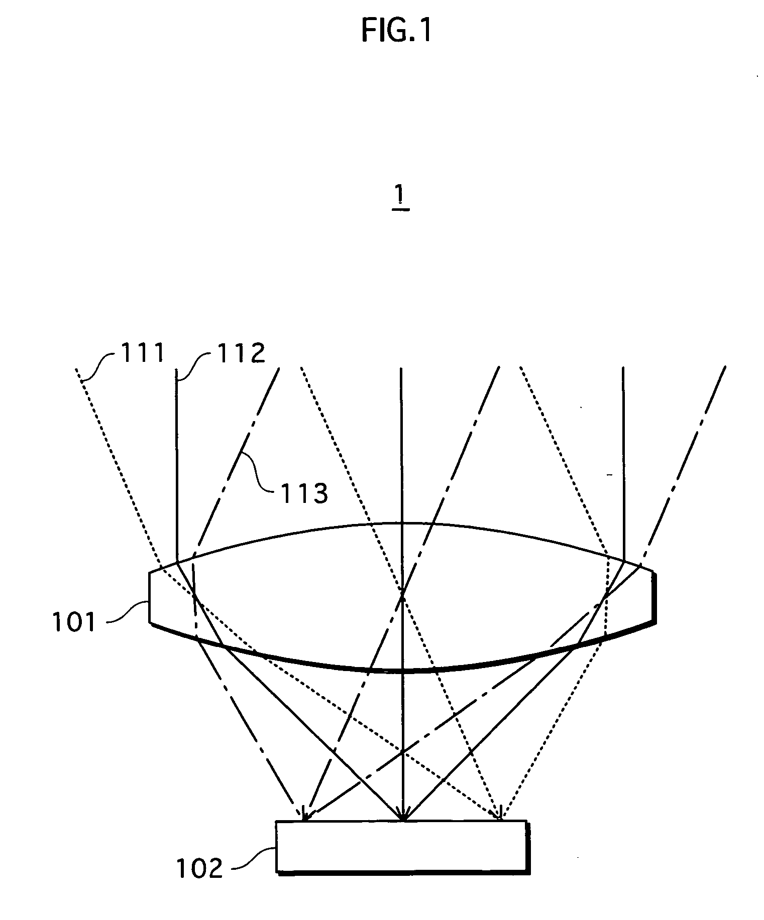
[0047] Firstly, the structure of a MOS image sensor pertaining to the present embodiment is described. FIG. 3 is a circuit diagram showing the main structure of a MOS image sensor pertaining to the present embodiment.

[0048] As shown in FIG. 3, MOS image sensor 3 is provided with an imaging area 310, a vertical shift register 321, a horizontal shift register 322, reset lines 323, horizontal pixel selection lines 324, vertical selection transistors 325, a horizontal signal line 327, and vertical voltage input transistors 328.

[0049] A large number of pixel cells are two dimensionally arrayed in imaging area 310. Individual pixel cells 311 a...

embodiment 2

[0074] A MOS image sensor pertaining to the present embodiment is provided with generally the same structure as a MOS image sensor pertaining to embodiment 1, except that the pitch of the metal layers for ensuring electrical connectivity (equivalent to metal layers 406B in embodiment 1) differs depending on location in the imaging area. The present embodiment is described below, focusing exclusively on this difference.

[0075] (1) Division of Imaging Area

[0076] In the present embodiment, the imaging area is divided into a plurality of sub-areas, with the pitch of the metal layers for ensuring electrical connectivity being the same within respective sub-areas. This pitch becomes smaller the further the sub-area is from the middle of the imaging area.

[0077]FIGS. 6A and 6B are schematic views showing an exemplary division of the imaging area. FIG. 6A shows an example of the imaging area divided by concentric circles centered on the middle of the imaging area, while FIG. 6B shows an ex...

embodiment 3

[0081] Next, an embodiment 3 of the present invention is described. A MOS image sensor pertaining to the present embodiment is provided with generally the same structure as a MOS image sensor pertaining to embodiment 1, except that the pitch of the metal layers for ensuring electrical connectivity (equivalent to metal layers 406B in embodiment 1) differs depending on location in the imaging area. The present embodiment is described below, focusing exclusively on this difference.

[0082] (1) Structure of Pixel Cells

[0083] Firstly, the structure of pixel cells provided in a MOS image sensor pertaining to the present embodiment is described.

[0084]FIGS. 8A to 8D show the structure of a pixel cell provided in a MOS image sensor pertaining to the present embodiment. FIGS. 8A and 8C are a plan view and a cross-sectional view of the pixel cell located in the middle of the imaging area, while FIGS. 8B and 8D are a plan view and a cross-sectional view of the pixel cell located at the periphe...


PUM


Abstract

A solid-state imaging device has a plurality of photoelectric conversion elements two dimensionally arrayed in an imaging area, a light shielding film that regulates the amount of external light incident on the photoelectric conversion elements by a wiring pattern, a wiring layer placed between the light shielding film and the photoelectric conversion elements, and a plurality of contacts electrically connecting the light shielding film with the wiring layer in a lamination direction. The shape of the light shielding film is defined by a plurality of first figures overlapping with a second figure, each first figure being placed over a different contact in plan view, and the second figure having a plurality of apertures each corresponding to a different photoelectric conversion element. The center of each aperture in the second figure is displaced further from the center of a corresponding photoelectric conversion element toward the middle of the imaging area in plan view, as distance from the middle of the imaging area increases. Furthermore, a positional relation of the first figures with the second figure differs depending on location in the imaging area.

Description

CROSS-REFERENCE TO RELATED APPLICATIONS [0001] This application is based on application no. 2005-050436 filed in Japan, the content of which is hereby incorporated by reference. BACKGROUND OF INVENTION [0002] 1. Field of the Invention [0003] The present invention relates to a solid-state imaging device, and more particularly to technology for reducing sensitivity shading. [0004] 2. Related Art [0005] Solid-state imaging devices, remarkably popularized in recent years, typically receive external light via an optical lens. [0006]FIG. 1 is a cross-sectional view of a digital camera illustrating the optical path of external light incident on a solid-state imaging device via an optical lens. As shown in FIG. 1, digital camera 1 is provided with an optical lens 101 and a solid-state imaging device 102, and external light 111 to 113 is incident on solid-state imaging device 102 via optical lens 101. [0007] External light 112 indicated by the solid line is incident substantially at the midd...

Claims


Application Information

Patent Timeline
Patent Type & Authority Applications(United States)
IPC IPC(8): H04N5/225H01L27/14H01L27/146H04N5/335H04N5/361H04N5/369H04N5/374
CPCH01L27/14621H01L27/14623H01L27/14627H01L27/14643H01L27/14818H04M1/0202
Inventor KATSUNO, MOTONARIMIYAGAWA, RYOUHEI
Owner COLLABO INNOVATIONS INC
Why Eureka
Try Eureka