Thermal infrared sensor and manufacturing method thereof

a technology of infrared sensors and manufacturing methods, applied in the field of thermal infrared sensors, can solve the problems of difficult formation of antireflection films and inability to prevent reflection

Active Publication Date: 2012-03-15
RICOH KK
View PDF19 Cites 36 Cited by
  • Summary
  • Abstract
  • Description
  • Claims
  • Application Information

AI Technical Summary

Benefits of technology

[0013]The present invention provides a thermal infrared sensor and a manufacturing method thereof, in which one or more of the above-described disadvantages are eliminated.
[0014]A preferred embodiment of the present invention provides a thermal infrared sensor and a manufacturing method thereof with which the reflection ratio of infrared rays can be reduced at the back surface of an infrared ray absorbing film, in a thermal infrared sensor that receives infrared rays from the back surface of the infrared ray absorbing film.

Problems solved by technology

However, as to the interface between the substrate 103 and the hollow space 104 and the interface between the hollow space 104 and the infrared ray absorbing film 105, it is difficult to form an antireflection film, and therefore reflection cannot be prevented.

Method used


Image

  • Thermal infrared sensor and manufacturing method thereof
  • Thermal infrared sensor and manufacturing method thereof
  • Thermal infrared sensor and manufacturing method thereof

Examples


Embodiment Construction

[0035]A description is given, with reference to the accompanying drawings, of embodiments of the present invention.

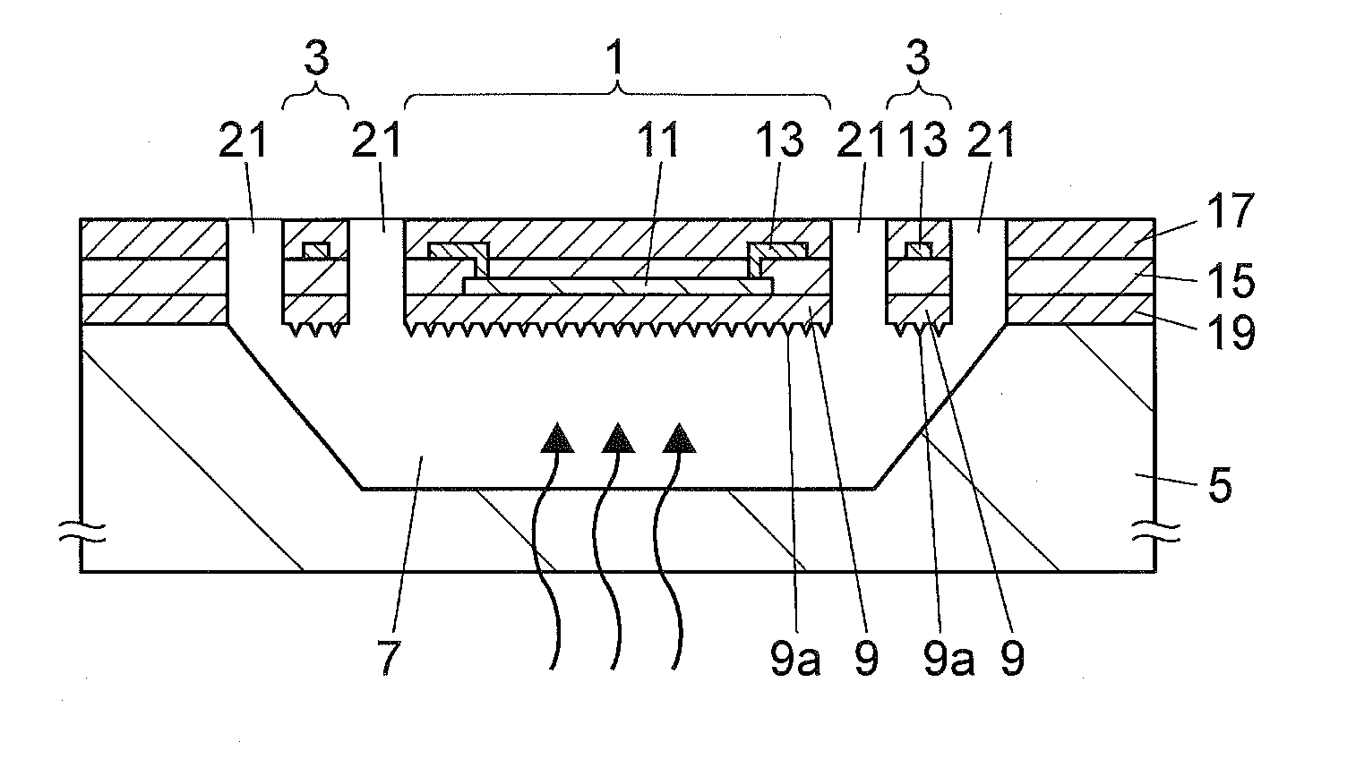
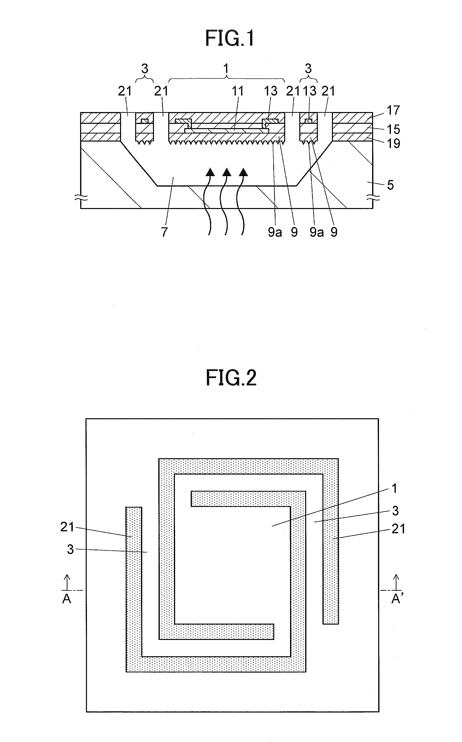
[0036]FIG. 1 is a schematic cross-sectional view of a thermal infrared sensor according to one embodiment. FIG. 2 is a schematic plan view of the embodiment illustrated in FIG. 1. FIG. 1 is a cross-sectional view cut along a line A-A′ in FIG. 2.

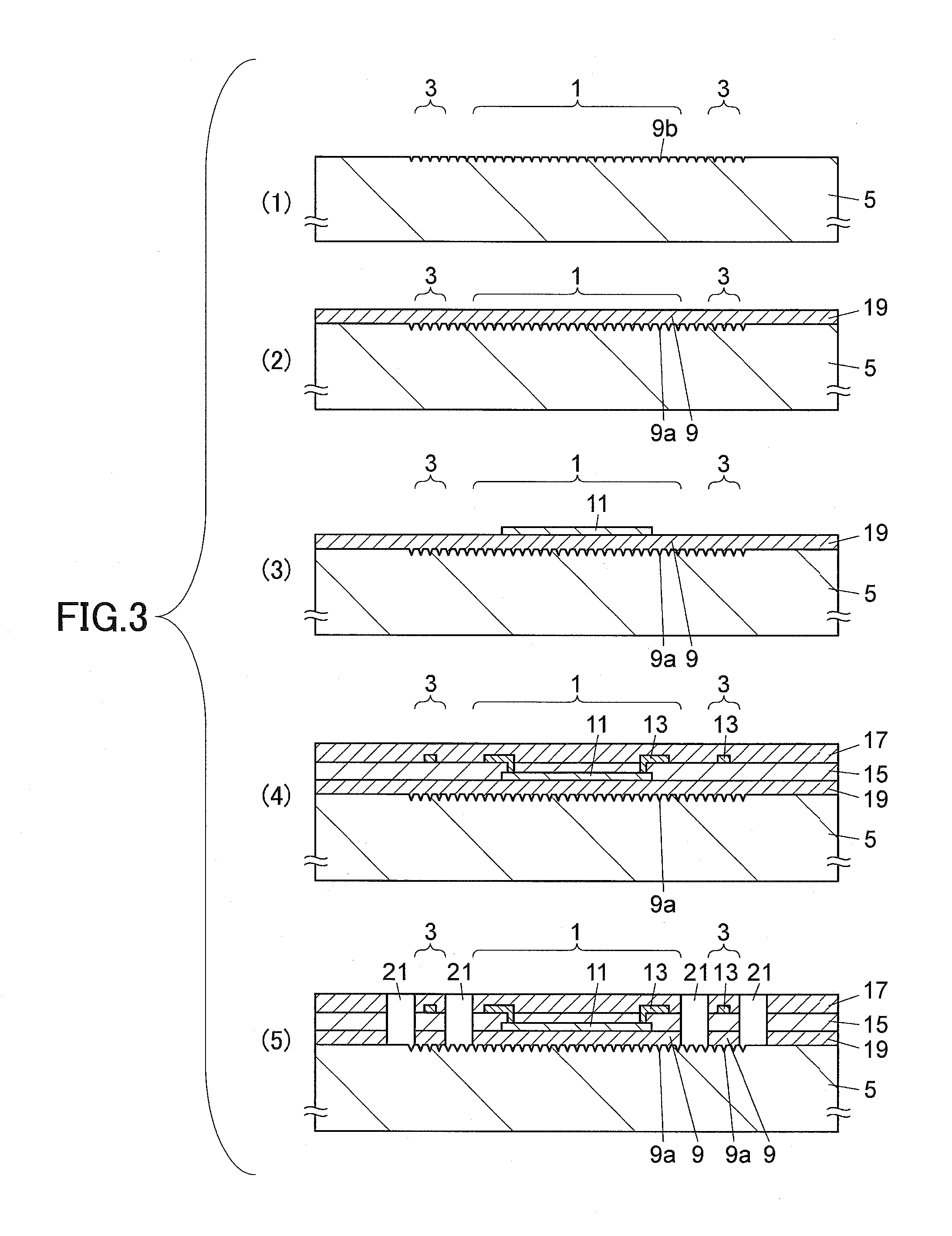
[0037]A sensor part 1 supported by beam parts 3 is facing a silicon substrate (semiconductor substrate) 5 across a hollow space 7. The sensor part 1 includes an infrared ray absorbing film 9, a temperature sensor 11, wirings 13, an interlayer insulating film 15, and a protection film 17. The beam parts 3 include the infrared ray absorbing film 9, the wirings 13, the interlayer insulating film 15, and the protection film 17.

[0038]The infrared ray absorbing film 9 is formed with a silicon oxide film. The infrared ray absorbing film 9 is thermally separated from the silicon substrate 5 by the hollow space 7. The infrared ray absorbi...


PUM


Abstract

A thermal infrared sensor includes an infrared ray absorbing film that is thermally separated from a semiconductor substrate by a hollow part; and a temperature sensor configured to detect temperature changes of the infrared ray absorbing film. The infrared ray absorbing film includes an infrared ray antireflection structure configured with a sub wavelength structure, the infrared ray antireflection structure being provided on a surface of the infrared ray absorbing film facing the semiconductor substrate.

Description

BACKGROUND OF THE INVENTION[0001]1. Field of the Invention[0002]The present invention relates to a thermal infrared sensor and a manufacturing method thereof, and more particularly to a thermal infrared sensor and a manufacturing method thereof for receiving infrared rays from the back surface of a substrate.[0003]2. Description of the Related Art[0004]There is a technology for increasing the sensitivity of a thermal infrared sensor such as a thermal infrared image sensor. Specifically, a bridge structure is formed by removing part of the substrate around the infrared ray absorbing film by etching to thermally separate the infrared ray absorbing film and the substrate. There is known a thermal infrared sensor configured to receive infrared rays at the back surface (substrate side) of the infrared ray absorbing film that is supported in a thermally insulated manner.[0005]For example, patent document 1 discloses a thermal infrared sensor in which an infrared ray absorbing film, a temp...

Claims


Application Information

Patent Timeline
Patent Type & Authority Applications(United States)
IPC IPC(8): G01J5/02H01L21/311
CPCG01J5/024G01J5/0853G01J5/0881
Inventor NOGUCHI, HIDETAKA
Owner RICOH KK
Why Eureka
Try Eureka